Multi-chip intelligent mounting equipment and using method thereof

A multi-chip, intelligent technology, applied in the manufacturing of electrical components, electric solid-state devices, semiconductor/solid-state devices, etc., can solve the problems of large footprint, insufficient speed, poor integration, etc., to reduce the equipment footprint , Easy to operate, ensure the effect of placement quality

Pending Publication Date: 2020-11-03
恩纳基智能科技无锡有限公司
View PDF0 Cites 6 Cited by
  • Summary
  • Abstract
  • Description
  • Claims
  • Application Information

AI Technical Summary

Problems solved by technology

[0003] The placement machine accuracy and UPH (capacity per hour) in the prior art are often not compatible. The placement machine that can achieve ±7 micron accuracy is not fast enough, and the UPH is only between 400 and 500; while the UPH reaches 1500 The precision of the placement machine is only ±10 microns; on the other hand, because chip production is extremely demanding on the environment and requires a 100-level workshop, manufacturers usually prefer relatively small placement equipment, while the existing Due to poor integration, the placement machine is relatively large in size and occupies a large area

Method used


Image

  • Multi-chip intelligent mounting equipment and using method thereof
  • Multi-chip intelligent mounting equipment and using method thereof
  • Multi-chip intelligent mounting equipment and using method thereof

Examples


Embodiment Construction

[0058] The specific implementation manner of the present invention will be described below in conjunction with the accompanying drawings.

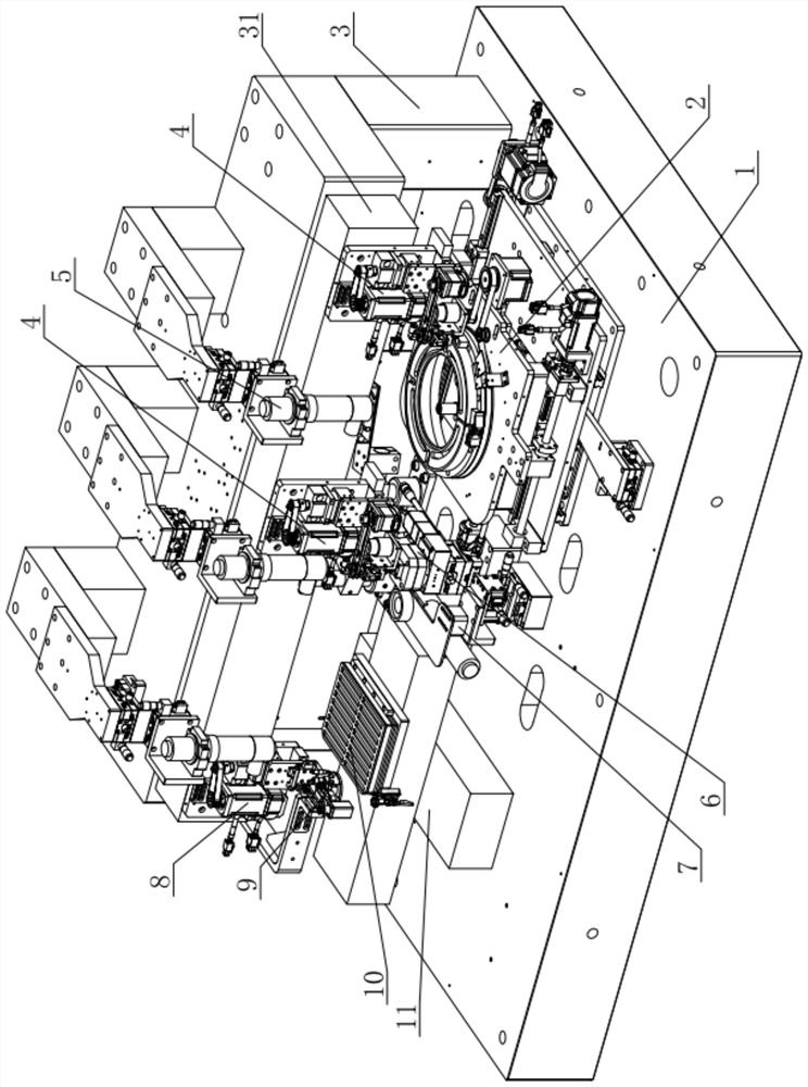
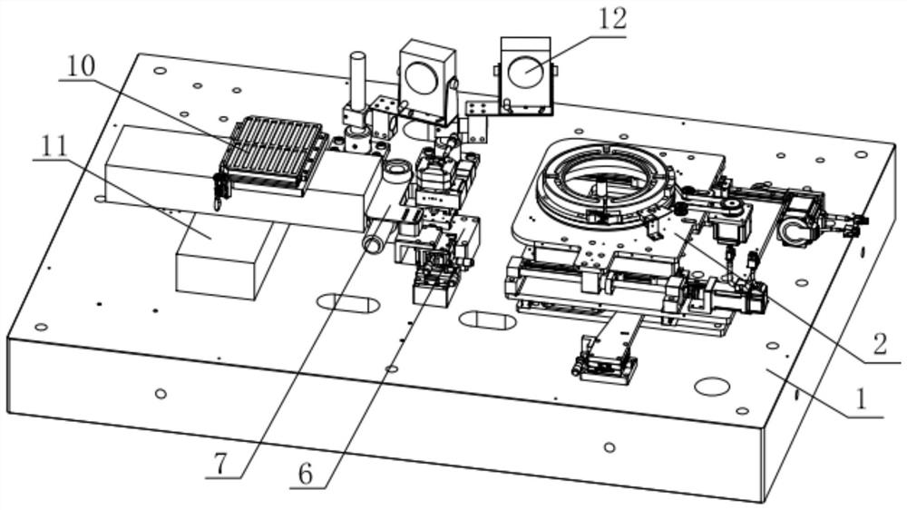
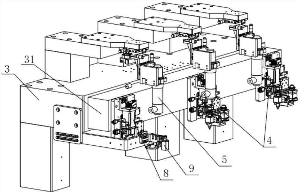
[0059] Such as figure 1 , figure 2 and image 3 As shown, the multi-chip intelligent placement equipment of this embodiment includes a working platform 1, on which a loading area 2, a preset platform 6 and a loading area 10 are arranged in sequence along the Y-axis direction, and are located in the loading area 2. A support frame 3 is installed on the working platform 1 outside the preset platform 6 and the end of the blanking area 10, and the front side of the support frame 3 is installed with a Y-direction linear guide rail 31 along the length direction, and the Y-direction linear guide rail 31 is moved and installed There is a welding head assembly 4, and a gluing assembly 8 is installed on the Y-direction linear guide rail 31 above the unloading area 10; multiple groups of camera assemblies 15 are installed on the top of the support...


PUM


Abstract

The invention relates to multi-chip intelligent mounting equipment and a using method thereof. The multi-chip intelligent mounting equipment comprises a working platform, wherein a feeding area, a preset platform and a discharging area are sequentially arranged on the working platform in the Y-axis direction, a supporting frame is installed on the working platform located outside the ends of the feeding area, the preset platform and the discharging area, and a Y-direction linear guide rail is installed on the front side face of the supporting frame in the length direction; a welding head assembly is movably installed on the Y-direction linear guide rail, and a gluing assembly is further installed on the Y-direction linear guide rail located above the discharging area. A plurality of firstcamera assemblies are further installed at the top of the supporting frame, and second camera assemblies are installed on the working platform located on the front side of the preset platform. One setof welding head assembly picks up the chips in the feeding area to the preset platform, the other set of welding head assembly picks up the chips on the preset platform to the discharging area, and the substrate in the discharging area is glued by the gluing assembly before the chips are placed, so high-precision mounting of the wafers on the substrate is realized, the automation degree is high,the mounting efficiency is greatly improved, and the surface mounting quality is guaranteed.

Description

technical field [0001] The invention relates to the technical field of chip assembly, in particular to a multi-chip intelligent mounting device and a method for using the same. Background technique [0002] In the chip manufacturing process, it is usually necessary to attach the wafers arranged in an orderly manner on the wafer ring to the substrate, and there is a large viscosity between the wafer and the blue film of the wafer ring, and the wafer needs to be removed from the Remove the wafer from the ring, apply glue to the substrate, and then stick the removed wafer to the glue-coated substrate. [0003] The placement machine accuracy and UPH (capacity per hour) in the prior art are often not compatible. The placement machine that can achieve ±7 micron accuracy is not fast enough, and the UPH is only between 400 and 500; while the UPH reaches 1500 The precision of the placement machine is only ±10 microns; on the other hand, because chip production is extremely demanding...

Claims


Application Information

Patent Timeline
Patent Type & Authority Applications(China)
IPC IPC(8): H01L21/67H01L21/68H01L21/60
CPCH01L21/67144H01L21/681H01L24/75H01L24/83H01L2224/75001H01L2224/7515H01L2224/75753H01L2224/75804H01L2224/83024H01L2224/83121
Inventor 吴超曾义徐金万汪凡姜超
Owner 恩纳基智能科技无锡有限公司
Why Eureka
Try Eureka