Light emitting diode chip and preparation method thereof

A technology of light-emitting diodes and chips, applied in electrical components, circuits, semiconductor devices, etc., can solve the problems of low light-emitting efficiency of LED chips, and achieve the effects of avoiding losses, increasing front-side light-emitting, and maintaining surface area.

Active Publication Date: 2020-11-03
HC SEMITEK SUZHOU
View PDF9 Cites 0 Cited by
  • Summary
  • Abstract
  • Description
  • Claims
  • Application Information

AI Technical Summary

Problems solved by technology

In the light emitted by the active layer, the light emitted from the side where the N-type electrode and the P-type electrode are located (called the front side of the chip) is used, but the light output efficiency of the front side of the LED chip is low

Method used


Image

  • Light emitting diode chip and preparation method thereof
  • Light emitting diode chip and preparation method thereof
  • Light emitting diode chip and preparation method thereof

Examples


Embodiment Construction

[0028] In order to make the purpose, technical solution and advantages of the present disclosure clearer, the implementation manners of the present disclosure will be further described in detail below in conjunction with the accompanying drawings.

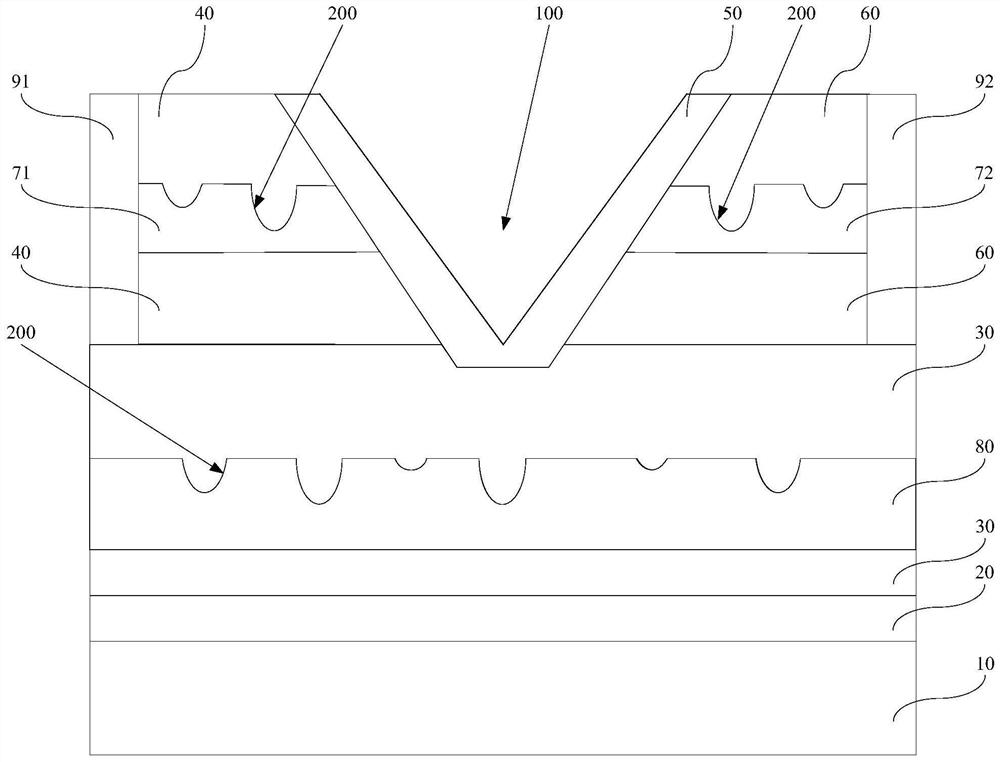
[0029] An embodiment of the disclosure provides a light emitting diode chip. figure 1 A schematic structural diagram of a light emitting diode chip provided by an embodiment of the present disclosure. see figure 1 , the LED chip includes a substrate 10 , a buffer layer 20 , an undoped gallium nitride layer 30 , an N-type semiconductor layer 40 , an active layer 50 , a P-type semiconductor layer 60 , an N-type electrode 91 and a P-type electrode 92 . The buffer layer 20 is laid on the substrate 10 , and the undoped gallium nitride layer 30 is laid on the buffer layer 20 . The N-type semiconductor layer 40 and the P-type semiconductor layer 60 are spaced apart on the undoped GaN layer 30 . A groove 100 is formed between the N-type...


PUM

PropertyMeasurementUnit
depthaaaaaaaaaa
thicknessaaaaaaaaaa
thicknessaaaaaaaaaa

Abstract

The invention provides a light emitting diode chip and a preparation method thereof, and belongs to the technical field of semiconductors. The light emitting diode chip comprises a substrate, a bufferlayer, an undoped gallium nitride layer, an N-type semiconductor layer, an active layer, a P-type semiconductor layer, an N-type electrode and a P-type electrode. The buffer layer is laid on the substrate, and the undoped gallium nitride layer is laid on the buffer layer; the N-type semiconductor layer and the P-type semiconductor layer are arranged on the undoped gallium nitride layer at intervals; a groove is formed between the N-type semiconductor layer and the P-type semiconductor layer, and the groove is in the shape of an inverted trapezoidal prism; the active layer is laid on the innerwall of the groove; the N-type electrode is arranged on the N-type semiconductor layer, and the P-type electrode is arranged on the P-type semiconductor layer. According to the invention, the front light emitting efficiency of an LED chip can be improved.

Description

technical field [0001] The present disclosure relates to the technical field of semiconductors, in particular to a light emitting diode chip and a preparation method thereof. Background technique [0002] LED (English: Light Emitting Diode, Chinese: Light Emitting Diode) is a semiconductor electronic device that can emit light. The chip is the core device of the LED, and currently it is mainly formed of gallium nitride-based materials. [0003] In related technologies, an LED chip includes a substrate, a buffer layer, an undoped gallium nitride layer, an N-type semiconductor layer, an active layer, a P-type semiconductor layer, an N-type electrode, and a P-type electrode. The buffer layer, the undoped gallium nitride layer, the N-type semiconductor layer, the active layer, and the P-type semiconductor layer are sequentially stacked on the substrate. The P-type semiconductor layer is provided with a groove extending to the N-type semiconductor layer. The electrodes are arra...

Claims


Application Information

Patent Timeline
Patent Type & Authority Applications(China)
IPC IPC(8): H01L33/20H01L33/24H01L33/00
CPCH01L33/007H01L33/20H01L33/24
Inventor 王群郭磊磊葛永晖董彬忠李鹏王江波
Owner HC SEMITEK SUZHOU
Why Eureka
Try Eureka