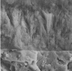
Wear-resistant mold surface nanocrystal coating and preparation method thereof
A nano-crystal, wear-resistant technology, applied in the coating, metal material coating process, fusion spraying, etc., can solve the problem of the mold is not wear-resistant, to avoid mold wear, reduce friction, high-quality surface The effect of finish
- Summary
- Abstract
- Description
- Claims
- Application Information
AI Technical Summary
Problems solved by technology
Method used
Image
Examples
Example Embodiment
[0027] Example 1
[0028] The present invention provides methods such as Figure 1 The nano-crystal layer on the surface of the wear-resistant mold shown in the figure consists of TiN crystal phase as the bottom layer, TiCN crystal phase +TiC crystal phase as the transition layer and Al.2 O 3 The crystal phase is composed of wear-resistant layer, in which TiCN crystal is dispersed in TiC crystal phase, TiN crystal phase is bonded with TiC crystal phase +TiC crystal phase, and TiC crystal phase +TiC crystal phase is Al. 2 O 3 Crystal phase bonding;
[0029] The thickness of the bottom layer is 2um;;
[0030] The thickness of the transition layer is 7um;;
[0031] The thickness of the wear-resistant layer is 3um.
[0032] In this embodiment, specifically, the total thickness of the nanocrystal layer is 12um.
[0033] In this embodiment, the bottom layer is located on one side close to the surface of the mold, and the transition layer is located between the bottom layer and the wear-r...
Example Embodiment
[0044] Example 2
[0045] The present invention provides methods such as Figure 1 The nano-crystal layer on the surface of the wear-resistant mold shown is different from the first embodiment in that the TiN crystal phase is the bottom layer, the TiCN crystal phase +TiC crystal phase is the transition layer and Al. 2 O 3 The crystal phase is composed of wear-resistant layer, in which TiCN crystal is dispersed in TiC crystal phase, TiN crystal phase is bonded with TiC crystal phase +TiC crystal phase, and TiC crystal phase +TiC crystal phase is Al. 2 O 3 Crystal phase bonding;
[0046] The thickness of the bottom layer is 3um;;
[0047] The thickness of the transition layer is 6um;;
[0048] The thickness of the wear-resistant layer is 4um.
[0049] In this embodiment, specifically, the total thickness of the nanocrystal layer is 13um.
[0050] In this example, specifically, the grain size range of the TiN crystal phase is 105nm, the grain size range of the TiCN crystal phase is 11...
Example Embodiment
[0056] Example 3
[0057] The present invention provides methods such as Figure 1 The nano-crystal layer on the surface of the wear-resistant mold shown is different from the first embodiment in that the TiN crystal phase is the bottom layer, the TiCN crystal phase +TiC crystal phase is the transition layer and Al. 2 O 3 The crystal phase is composed of wear-resistant layer, in which TiCN crystal is dispersed in TiC crystal phase, TiN crystal phase is bonded with TiC crystal phase +TiC crystal phase, and TiC crystal phase +TiC crystal phase is Al. 2 O 3 Crystal phase bonding;
[0058] The thickness of the bottom layer is 3um;;
[0059] The thickness of the transition layer is 7um;;
[0060] The thickness of the wear-resistant layer is 5um.
[0061] In this embodiment, specifically, the total thickness of the nanocrystal layer is 15um.
[0062] In this embodiment, specifically, the grain size range of TiN crystal phase is 75-150nm, the grain size range of TiCN crystal phase is 140n...
PUM
| Property | Measurement | Unit |
|---|---|---|
| Thickness | aaaaa | aaaaa |
| Thickness | aaaaa | aaaaa |
| Thickness | aaaaa | aaaaa |
Abstract
Description
Claims
Application Information
