

Vapor deposition chamber
A vapor deposition and chamber technology, applied in electrical components, from chemically reactive gases, crystal growth, etc., can solve the problems of space pollution below, difficulty of etching gas entering the space below, and affecting machine start-up rate, etc., to improve performance , The effect of reducing maintenance time
- Summary
- Abstract
- Description
- Claims
- Application Information
AI Technical Summary
Problems solved by technology
Method used
Image

Examples
Embodiment Construction
[0027] In order to make the purpose, technical solution and advantages of the present application clearer, the technical solution of the present application will be clearly and completely described below in conjunction with specific embodiments of the present application and corresponding drawings. Apparently, the described embodiments are only some of the embodiments of the present application, rather than all the embodiments. Based on the embodiments in this application, all other embodiments obtained by persons of ordinary skill in the art without making creative efforts belong to the scope of protection of this application.
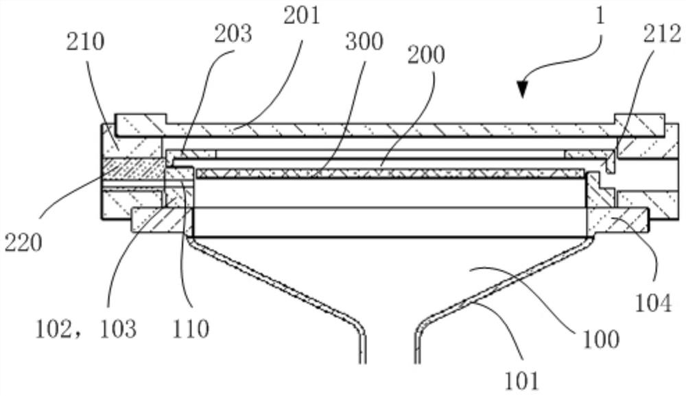
[0028] figure 1 The structure of a vapor deposition chamber 1 according to an embodiment of the present application is schematically shown.
[0029] Such as figure 1 As shown, the vapor deposition chamber 1 includes a first sub-chamber 100 and a second sub-chamber 200 . The first sub-chamber 100 and the second sub-chamber 200 are separated in the...
PUM
 Abstract
Description
Claims
Application Information