Artwork display screen and manufacturing method thereof

A manufacturing method and display screen technology, which are applied in semiconductor/solid-state device manufacturing, identification devices, instruments, etc., can solve problems such as cracking and damage, and achieve the effects of preventing peeling, increasing bonding stability, and improving service life

Active Publication Date: 2022-04-12
ZIBO VOCATIONAL INST
View PDF12 Cites 0 Cited by
  • Summary
  • Abstract
  • Description
  • Claims
  • Application Information

AI Technical Summary

Problems solved by technology

The existing art display screen is prone to cracking and damage during use

Method used


Image

  • Artwork display screen and manufacturing method thereof
  • Artwork display screen and manufacturing method thereof
  • Artwork display screen and manufacturing method thereof

Examples


Embodiment Construction

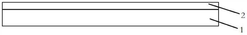
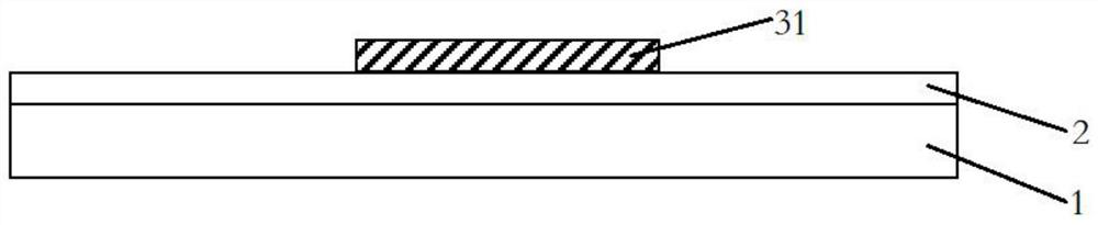
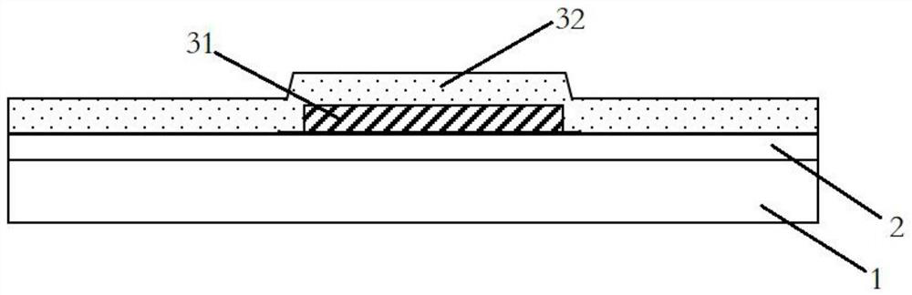
[0028] In order to make the purpose, technical solutions and advantages of the embodiments of the present invention clearer, the technical solutions in the embodiments of the present invention will be clearly and completely described below in conjunction with the drawings in the embodiments of the present invention. Obviously, the described embodiments It is only some embodiments of the present invention, but not all embodiments. Based on the embodiments of the present invention, all other embodiments obtained by persons of ordinary skill in the art without making creative efforts belong to the protection scope of the present invention. The terms "first", "second", "third", etc. (if any) in the description and claims of the present invention and the above drawings are used to distinguish similar objects and not necessarily to describe a specific order or sequentially. It is to be understood that the data so used are interchangeable under appropriate circumstances such that th...


PUM


Abstract

The present invention relates to an artwork display screen and a manufacturing method thereof, the method comprising: depositing a buffer layer, a semiconductor active layer, a gate insulating layer, a gate layer and an interlayer dielectric layer on the base substrate, and then depositing The interlayer dielectric layer in the edge area of ​​the display panel is etched to form a first groove surrounding the pixel area of ​​the display panel, and then a second groove is formed on the bottom surface of the first groove, Next, metal material is deposited in the first groove and the second groove to form a metal bump, and then a third groove is formed on the upper surface of the metal bump; then, in the interlayer dielectric layer A planarization layer is formed on the planarization layer, and then an anode layer, a light emitting layer and a cathode layer are formed on the planarization layer.

Description

technical field [0001] The invention relates to the technical field of semiconductor packaging, in particular to an artwork display screen and a manufacturing method thereof. Background technique [0002] Existing art display screens usually use organic light emitting diode display panels as their main parts, and the organic light emitting diode display panels have the advantages of self-illumination, fast response, wide viewing angle, and simple manufacture. In the preparation process of the existing OLED display panel, a buffer layer, a semiconductor active layer, a gate insulating layer, a gate, an interlayer dielectric layer, a source drain, a planarization layer, and an organic LED unit. The existing art display screen is prone to cracking and damage during use. Contents of the invention [0003] The purpose of the present invention is to overcome the shortcomings of the above-mentioned prior art, and provide an art display screen and a manufacturing method thereof....

Claims


Application Information

Patent Timeline
Patent Type & Authority Patents(China)
IPC IPC(8): H01L27/32H01L27/12H01L21/77G09F9/33
CPCH01L27/1248H01L27/124G09F9/33H10K59/124H10K59/131H10K59/1201
Inventor 孙波
Owner ZIBO VOCATIONAL INST
Why Eureka
Try Eureka