

Semiconductor device
A technology for semiconductors and structural components, applied in the fields of semiconductor devices, semiconductor/solid-state device manufacturing, semiconductor/solid-state device components, etc.
- Summary
- Abstract
- Description
- Claims
- Application Information
AI Technical Summary
Problems solved by technology
Method used
Image

Examples
Embodiment approach 1
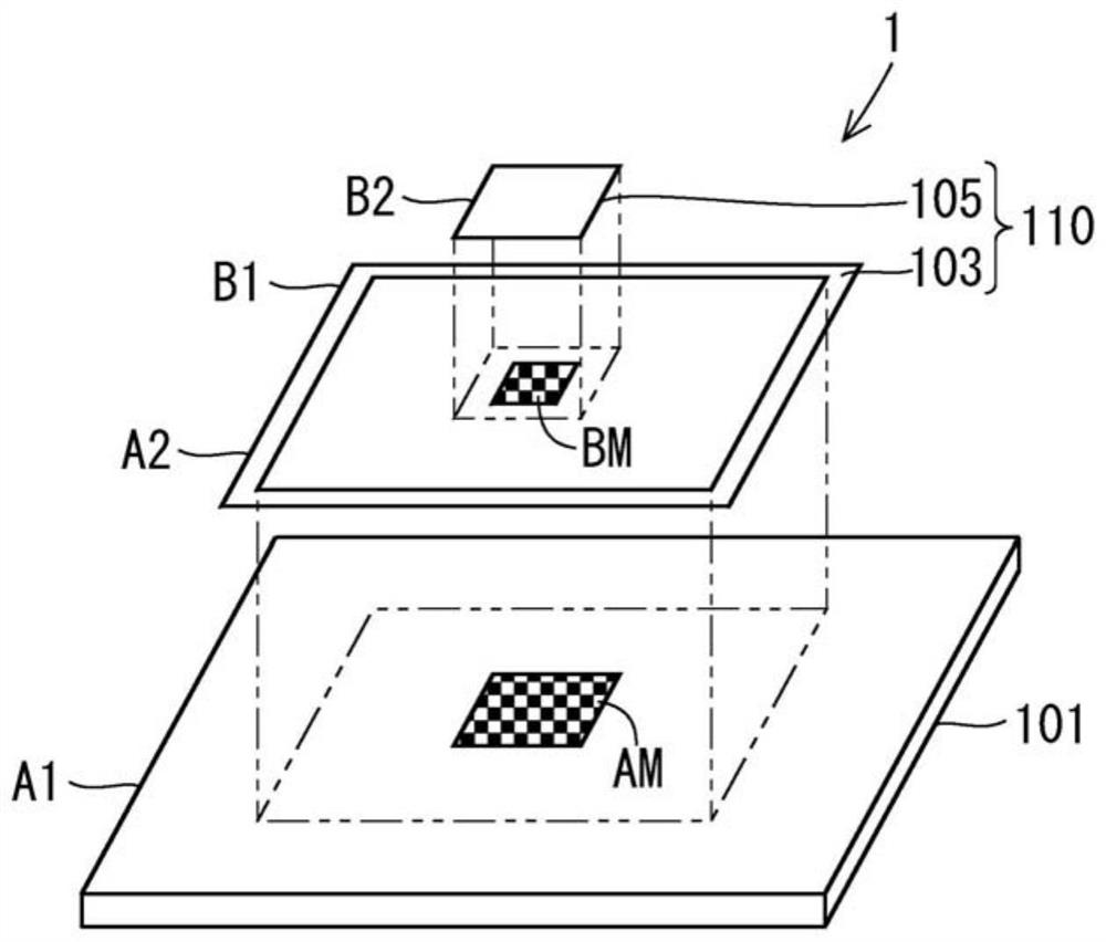
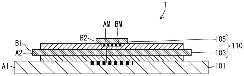
[0026] 1.1 Semiconductor device
[0027] figure 1 It is an exploded perspective view schematically illustrating the semiconductor device of Embodiment 1. FIG. figure 2 It is a cross-sectional view schematically illustrating the semiconductor device of the first embodiment.
[0028] figure 1 as well as figure 2 The illustrated semiconductor device 1 of Embodiment 1 is a power module.
[0029] The semiconductor device 1 may be a semiconductor device other than a power module.
[0030] The semiconductor device 1 has a structural component 101 and a plurality of structural components 110 . A plurality of structural components 110 are mounted and stacked on the structural component 101 .
[0031] The structural member 101 is a base substrate serving as a reference. The structural component 101 may also be a structural component other than the base substrate.
[0032] The plurality of structural components 110 has structural components 103 and structural components 105 . ...
Embodiment approach 2
[0064] Figure 4 It is an exploded perspective view schematically showing the semiconductor device of Embodiment 2. Figure 5 It is a cross-sectional view schematically illustrating a semiconductor device according to Embodiment 2.
[0065] Figure 4 as well as Figure 5 The illustrated semiconductor device 2 of Embodiment 2 and figure 1 as well as figure 2 The illustrated semiconductor device 1 of Embodiment 1 is mainly different in the following points. Regarding points not described below, the semiconductor device 2 of the second embodiment also has the same structure as that of the semiconductor device 1 of the first embodiment.
[0066] The plurality of structural components 110 includes a structural component 102 , a structural component 103 , a structural component 104 , and a structural component 105 .
[0067] The first structural member A1 has a structural member 101 . The second structural member A2 has two or more structural members 102 and 103 stacked. Th...
Embodiment approach 3
[0074] Figure 6 It is an exploded perspective view schematically illustrating the semiconductor device of Embodiment 3. Figure 7 It is a cross-sectional view schematically illustrating a semiconductor device according to Embodiment 3.
[0075] Figure 6 as well as Figure 7 The illustrated semiconductor device 3 of Embodiment 3 and figure 1 as well as figure 2 The illustrated semiconductor device 1 of Embodiment 1 is mainly different in the following points. Regarding points not described below, the semiconductor device 3 of the third embodiment also has the same structure as that of the semiconductor device 1 of the first embodiment. The semiconductor device 3 of the third embodiment can also be used with Figure 4 as well as Figure 5 The semiconductor device 2 of the illustrated second embodiment has the same structure as that adopted.
[0076] The semiconductor device 3 has a structural component 101 , a plurality of structural components 110P, and a plurality o...
PUM
 Abstract
Description
Claims
Application Information