Etching method

A technology to be etched and resistant to etching, which is applied in the manufacture of electrical components, circuits, semiconductors/solid-state devices, etc. It can solve the problems of easy pattern collapse, etc., and achieve reduced attenuation, strong etching resistance, and increased thickness selectivity Effect

Active Publication Date: 2021-01-29
南京晶驱集成电路有限公司
View PDF4 Cites 0 Cited by
  • Summary
  • Abstract
  • Description
  • Claims
  • Application Information

AI Technical Summary

Problems solved by technology

However, when the thickness of the photoresist exceeds 4 times the CD (critical dimension), the pattern of the photoresist is very prone to collapse
Therefore, in the process that requires small CD value and deep etching, the thickness selection of photoresist becomes a challenge

Method used


Image

  • Etching method
  • Etching method
  • Etching method

Examples


Embodiment Construction

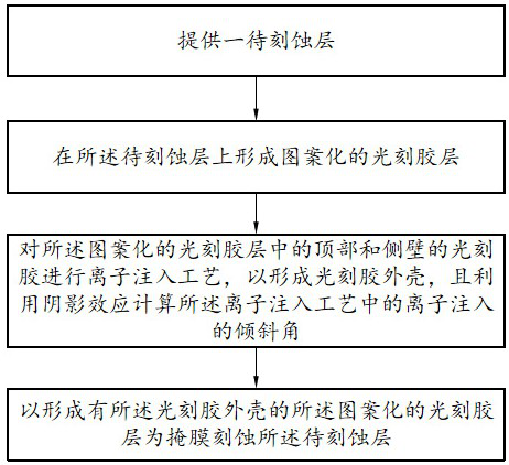
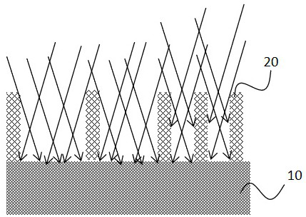
[0032] The etching method proposed by the present invention will be described in further detail below in conjunction with the accompanying drawings and specific embodiments. The advantages and features of the present invention will be more apparent from the following description. It should be noted that all the drawings are in a very simplified form and use imprecise scales, which are only used to facilitate and clearly assist the purpose of illustrating the embodiments of the present invention.

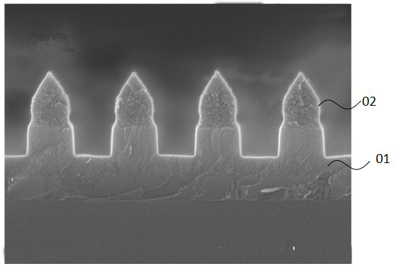
[0033] figure 1 The peaking phenomenon of photoresist is schematically shown. A patterned photoresist layer 02 is formed on the layer to be etched 01 , and the layer to be etched 01 is etched using the patterned photoresist layer 02 as a mask. Since the etching resistance of the photoresist is not strong, in the process of etching the layer 01 to be etched, the patterned photoresist layer 02 will also be etched a little, and attenuation occurs, while the The photoresist pattern of...


PUM


Abstract

The invention provides an etching method, comprising: firstly, providing a layer to be etched; then, forming a patterned photoresist layer on the layer to be etched; The photoresist on the top and sidewalls in the glue layer is subjected to an ion implantation process to form a photoresist shell, and the tilt angle θ of the ion implantation in the ion implantation process is calculated using the shadow effect; finally, to form the The patterned photoresist layer of the photoresist shell is used as a mask to etch the layer to be etched. The present invention forms a photoresist shell by performing an ion implantation process on the top and sidewall photoresist in the patterned photoresist layer, which can reduce the attenuation of the patterned photoresist layer during the etching process, and Increase thickness selectivity of photoresist.

Description

technical field [0001] The invention relates to the technical field of semiconductor manufacturing, in particular to an etching method. Background technique [0002] Etching is an important process in the preparation of semiconductor optoelectronic devices. Its purpose is to selectively remove materials from the surface of semiconductor material wafers by physical or chemical methods to form desired mesas or patterns. The etching process is divided into dry etching and wet etching. The pattern accuracy and anisotropy of dry etching are high, and the controllability of various parameters is good; wet etching has good repeatability, simple operation, fast etching rate, non-toxic or Low toxicity, good repeatability and other advantages. [0003] During the etching process, the area that does not need to be etched will be blocked by the photoresist, and the photoresist will also attenuate during the etching process, and the photoresist will produce a pointed shape due to the a...

Claims


Application Information

Patent Timeline
Patent Type & Authority Patents(China)
IPC IPC(8): H01L21/308H01L21/311H01L21/3213
CPCH01L21/3086H01L21/31144H01L21/32139
Inventor 程挚朱红波郭宜婷李昌达方晓宇
Owner 南京晶驱集成电路有限公司
Why Eureka
Try Eureka