Laser annealing device

A laser annealing and laser technology, which is applied in semiconductor/solid-state device testing/measurement, electrical components, circuits, etc., can solve the problems of laser annealing depth layer fluctuation, wafer surface unevenness, etc.

Active Publication Date: 2020-11-17
北京中科镭特电子有限公司
View PDF4 Cites 1 Cited by
  • Summary
  • Abstract
  • Description
  • Claims
  • Application Information

AI Technical Summary

Problems solved by technology

[0004] The invention provides a laser annealing device, which is used to solve the problem that th

Method used


Image

  • Laser annealing device
  • Laser annealing device
  • Laser annealing device

Examples


Embodiment Construction

[0028] In order to make the purposes, technical solutions and advantages of the embodiments of the present invention clearer, the technical solutions in the embodiments of the present invention will be clearly and completely described below with reference to the accompanying drawings in the embodiments of the present invention. Obviously, the described embodiments It is only a part of the embodiments of the present invention, but not all of the embodiments. Based on the embodiments of the present invention, all other embodiments obtained by those of ordinary skill in the art without creative efforts shall fall within the protection scope of the present invention.

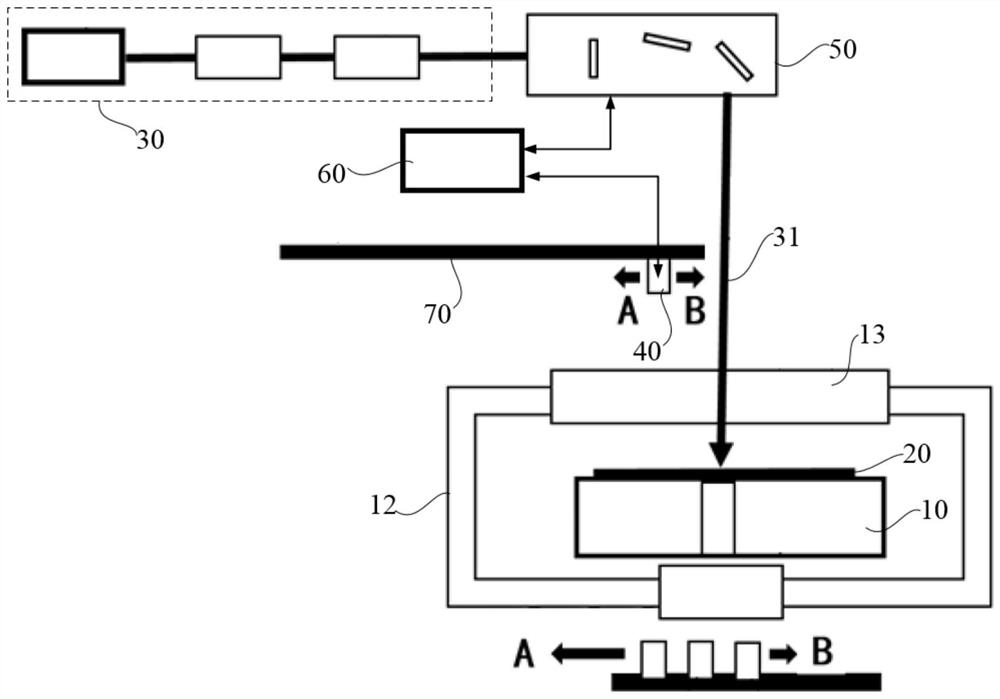
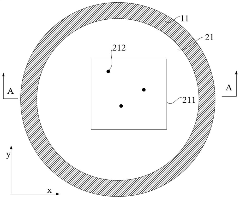
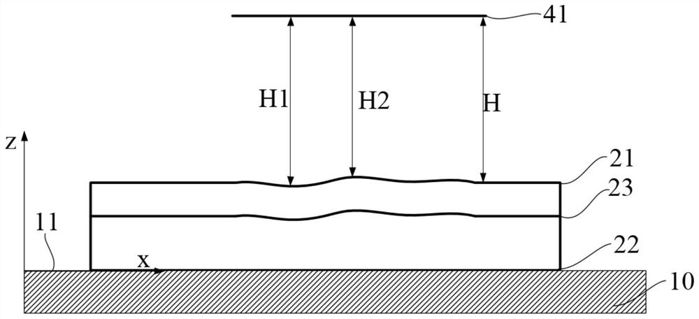
[0029] In order to facilitate the understanding of the laser annealing apparatus provided by the embodiment of the present invention, the following first describes the application scenario of the laser annealing apparatus provided by the embodiment of the present invention. The laser annealing apparatus is used for a...


PUM


Abstract

The invention provides a laser annealing device. The laser annealing device comprises an objective table for holding a wafer, a laser assembly for emitting a laser beam to the wafer to anneal the wafer, and the wafer is provided with a first surface deviating from the objective table and a second surface facing the objective table. The height indicator is arranged above the objective table, and the three-axis galvanometer system is arranged between the laser assembly and the wafer. The altimeter measures height difference changes between different positions on the first surface of the wafer and a reference surface set by the altimeter; the three-axis galvanometer system moves a laser beam emitted by the laser assembly to adjust the focus position of the laser beam focused on the wafer. Thethree-axis galvanometer system further comprises a control device, and the control device controls the three-axis galvanometer system to keep the focus on the layer structure, away from the first face by the set depth, of the wafer according to the height difference change measured by the altimeter. And the focus position of the laser beam is adjusted up and down according to the convex-concave fluctuation of the first surface of the wafer, so that the wafer annealing position accuracy is improved.

Description

technical field [0001] The present invention relates to the technical field of wafer manufacturing, in particular to a laser annealing device. Background technique [0002] With the progress and development of science and technology, laser has been used as a tool in all walks of life. Due to the characteristics of high brightness and high intensity of the laser, and the size of the laser focus can be focused to the micron level by the focusing mirror, laser processing technology is favored in industries with high precision processing requirements, especially for the semiconductor industry wafer manufacturing Among the technologies, laser processing technology is particularly popular. [0003] Initially, the annealing process of the wafers was carried out in a furnace containing a number of wafers supported in a holder. Electrical power is supplied to the resistive heater elements in the furnace walls to heat them to a temperature close to the desired process temperature. ...

Claims


Application Information

Patent Timeline
IPC IPC(8): H01L21/268H01L21/66H01L21/67
CPCH01L21/67115H01L21/268H01L21/67253H01L21/67288H01L22/12H01L22/26H01L22/24
Inventor 张昆鹏李纪东张紫辰侯煜易飞跃杨顺凯李曼张喆王然王瑜
Owner 北京中科镭特电子有限公司
Why Eureka
Try Eureka