Transparent wafer edge extraction method of pre-alignment machine

A pre-aligner and edge extraction technology, applied in the semiconductor field, can solve the problems of different light transmittance, difficult to calculate, unable to reflect the edge position of the transparent wafer, etc., to meet the sampling requirements, high precision, and low computational complexity. Effect

Active Publication Date: 2020-11-17
无锡卓海科技股份有限公司
View PDF6 Cites 0 Cited by
  • Summary
  • Abstract
  • Description
  • Claims
  • Application Information

AI Technical Summary

Problems solved by technology

[0004] However, different compound materials have different light transmittances. When inspecting compound wafers, since the material itself is light-transmitting, the light received by the pre-alignment machine is the light transmittance of the unshielded part of the wafer and the light transmittance of the wafer. The sum of the light transmission of the unshielded part is determined by the light source. This part is the same as that of the silicon wafer, but the light transmission of the wafer is related to various factors such as the material of the wafer itself, the wafer pattern, and the coating. Different angles It is difficult to accurately calculate the position and light transmission amount, so the edge position of the transparent wafer cannot be reflected only by the light reception amount

Method used


Image

  • Transparent wafer edge extraction method of pre-alignment machine
  • Transparent wafer edge extraction method of pre-alignment machine
  • Transparent wafer edge extraction method of pre-alignment machine

Examples


Embodiment Construction

[0031] The specific embodiments of the present invention will be further described below in conjunction with the accompanying drawings.

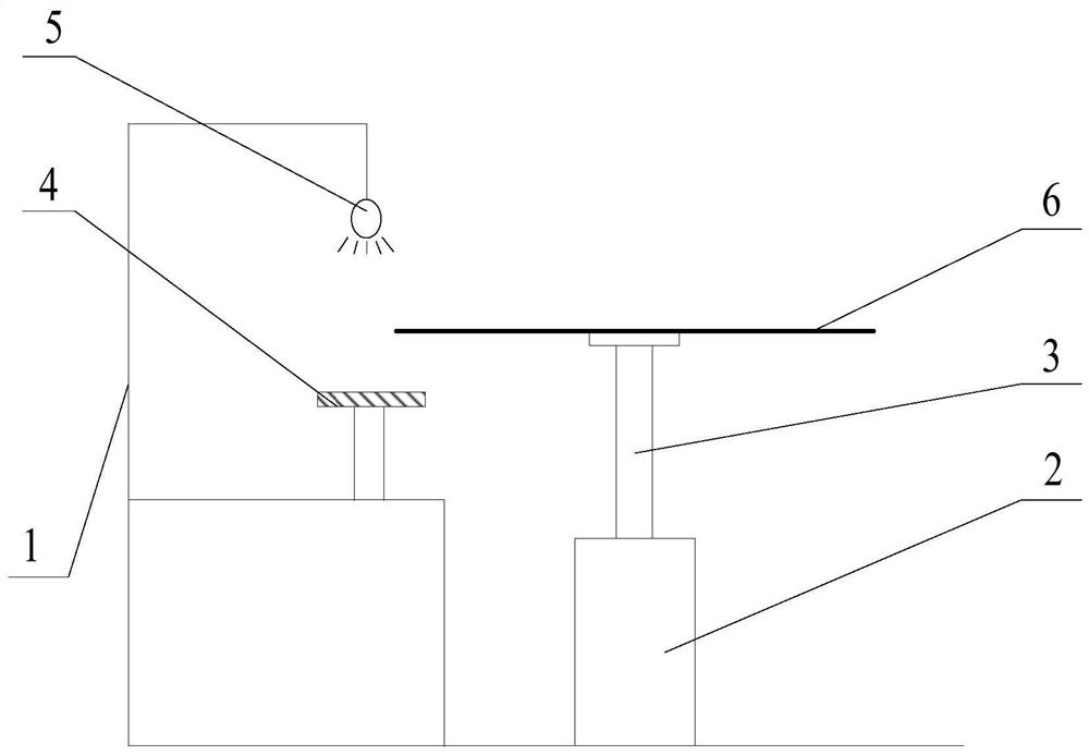
[0032] figure 1 Shows the principle block diagram of the pre-alignment machine to extract the edge of the wafer, the pre-alignment machine includes a pre-alignment support 1, a mobile platform 2, a rotating platform 3, a linear array CCD sensor 4 and a supporting light source 5, a linear array CCD sensor 4 and The matching light sources 5 are erected on the pre-alignment support 1 and placed opposite to each other in the center. The wafer is placed on the rotary platform 3, and the rotary platform 3 drives the wafer to rotate around the z-axis. The rotary platform 3 is provided with a vacuum air circuit for absorbing the wafer 6. The rotary platform 3 is placed on the mobile platform 2, and the mobile platform 2 drives the rotating platform 3 to move in the x-y direction, so that the wafer 6 moves between the linear CCD sensor 4 and the sup...


PUM


Abstract

The invention discloses a transparent wafer edge extraction method of a pre-alignment machine, and relates to the technical field of semiconductors, and the method comprises the steps: collecting first light receiving data of a linear array type CCD sensor when a wafer is not placed, and enabling the first light receiving data to serve as a light source reference waveform; placing a transparent wafer to be detected and controlling the mobile platform to move to the edge of the wafer to be located in the detection range of the linear array type CCD sensor; rotating the transparent wafer to be measured, collecting second light receiving data of the linear array type CCD sensor, and extracting edge data from the second light receiving data; carrying out the differential processing on the edgedata and the light source reference waveform, and obtaining the shading position of the linear array type CCD sensor through processing; performing edge compensation correction on the shading position to obtain a compensated shading position of the sensor; and converting the digital-to-analog signal and then outputting the signal to the pre-alignment machine to obtain the edge position of the transparent wafer to be measured. The edge compensation correction improves the accuracy of wafer edge extraction, and the extraction method enables the existing pre-alignment machine to support the edgeextraction of the transparent wafer.

Description

technical field [0001] The invention relates to the technical field of semiconductors, in particular to a transparent wafer edge extraction method for a pre-alignment machine. Background technique [0002] A wafer is a wafer with a single crystal structure. Different crystal orientations of wafers have different chemical, electrical and physical properties. The direction of the wafer is used as a reference, so the semiconductor equipment needs to locate the direction of the wafer before etching and measuring the wafer. Wafers have a notch or cut edge as a visible reference for crystal orientation, and semiconductor equipment recognizes the notch or cut edge of the wafer, and transfers the wafer at a specific angle to a precision mobile platform for processing and measurement. As the semiconductor process enters the nanometer level, the precision requirements for semiconductor equipment are getting higher and higher. In order to realize high-speed automatic production and me...

Claims


Application Information

Patent Timeline
Patent Type & Authority Applications(China)
IPC IPC(8): H01L21/68G03F9/00
CPCG03F9/7007G03F9/7049H01L21/681
Inventor 戴金方
Owner 无锡卓海科技股份有限公司
Why Eureka
Try Eureka