Electroplating system and method for BGA area in PCB

A PCB board and area technology, which is applied in the field of electroplating system in the BGA area of ​​the PCB board, can solve the problems of poor uniformity and low signal transmission performance in the PCB board

Active Publication Date: 2020-11-20
SUZHOU LANGCHAO INTELLIGENT TECH CO LTD
View PDF7 Cites 0 Cited by
  • Summary
  • Abstract
  • Description
  • Claims
  • Application Information

AI Technical Summary

Problems solved by technology

[0005] The present application provides an electroplating system and method for the BGA area in the PCB board, so as to solve the problem of low transmission performance and poor uniformity of signals in the PCB board caused by the methods in the prior art

Method used


Image

  • Electroplating system and method for BGA area in PCB
  • Electroplating system and method for BGA area in PCB
  • Electroplating system and method for BGA area in PCB

Examples


Embodiment 1

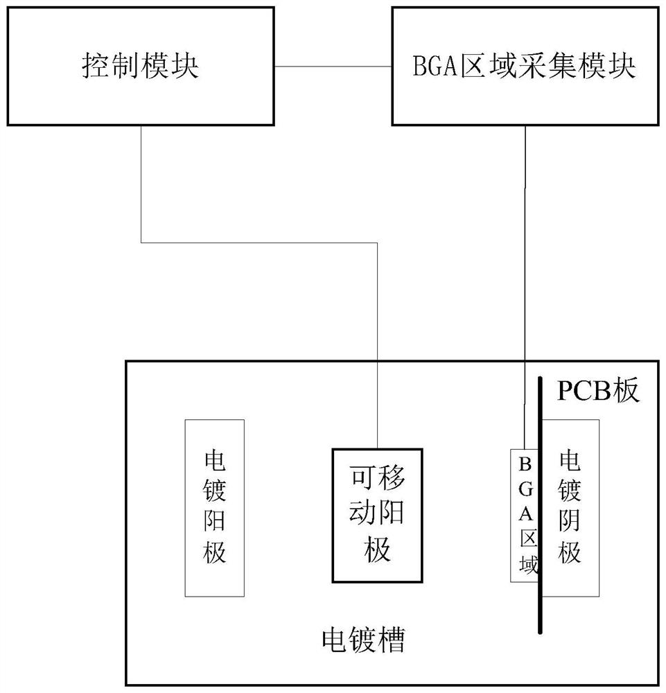
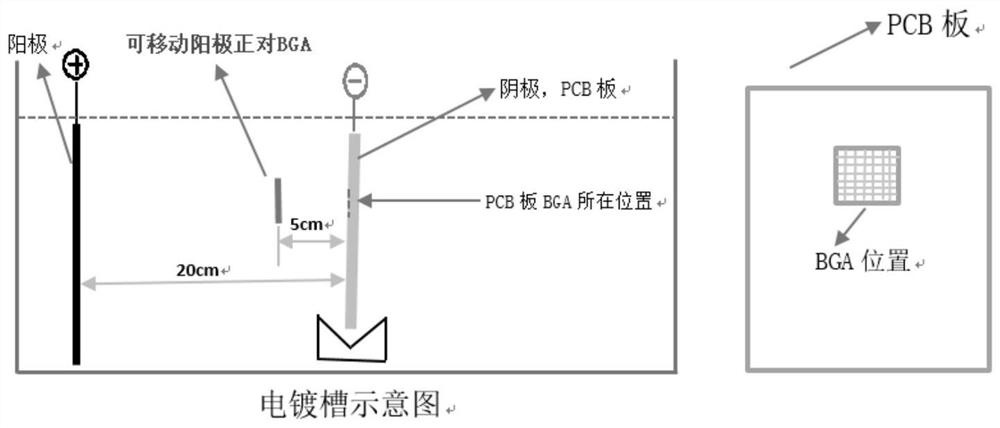
[0041] see figure 1 , figure 1 It is a schematic structural diagram of an electroplating system for a BGA area in a PCB board provided by an embodiment of the present application. Depend on figure 1 It can be seen that the electroplating system in the BGA area of ​​the PCB board in this embodiment mainly includes four parts: an electroplating tank, a BGA area acquisition module, a control module and a movable anode.

[0042]Among them, the electroplating tank is provided with electroplating anode and electroplating cathode, the electroplating anode is parallel to the electroplating cathode, the PCB board is placed on the electroplating cathode, the movable anode is parallel to the electroplating cathode, and the vertical distance between the movable anode and the electroplating cathode is less than the electroplating cathode. The vertical distance between the anode and the plating cathode. The BGA area acquisition module is used to identify and record the BGA area on the PC...

Embodiment 2

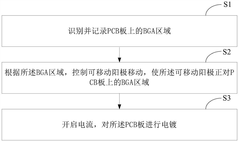
[0052] exist figure 1 and figure 2 On the basis of the illustrated embodiment see image 3 , image 3 It is a schematic flowchart of a method for electroplating a BGA area in a PCB board provided by an embodiment of the present application. Depend on image 3 It can be seen that the electroplating method of the BGA area in the PCB board of this embodiment mainly includes the following processes:

[0053] S1: Identify and record the BGA area on the PCB. Specifically, step S1 includes:

[0054] S11: Collect the arrangement of BGA holes on the PCB, and the BGA holes are used to install the CPU.

[0055] In this embodiment, the camera can be used to capture the layout of the BGA holes on the PCB.

[0056] S12: Identify the BGA area according to the arrangement of the collected BGA holes.

[0057] Specifically, step S12 includes the following processes:

[0058] S121 : According to the arrangement of the collected BGA holes, it is judged whether the number of holes in the...


PUM


Abstract

The invention discloses an electroplating system and method for a BGA area in a PCB. The system comprises an electroplating bath, a BGA area acquisition module, a control module and a movable anode. The PCB is placed on an electroplating cathode, and the vertical distance between the movable anode and the electroplating cathode is smaller than the vertical distance between an electroplating anodeand the electroplating cathode; the BGA area acquisition module is used for identifying and recording the BGA area on the PCB; and the control module is used for controlling the movable anode to moveto directly face the BGA area on the PCB according to the BGA area. The method comprises the following steps of identifying and recording the BGA area on the PCB, controlling the movable anode to moveaccording to the BGA area, enabling the movable anode to directly face the BGA area on the PCB, and starting current to electroplate the PCB. On the condition that the copper plating thickness of theBGA area meets the requirement, the problems of low signal transmission performance and poor uniformity caused by the increase of the thickness of the PCB are avoided, and the electroplating efficiency is improved.

Description

technical field [0001] The present application relates to the technical field of PCB (Printed Circuit Board, printed circuit board) board manufacturing, and in particular to an electroplating system and method for a BGA (Ball Grid Array Package, ball grid array package) area in a PCB board. Background technique [0002] The PCB board of the server is used to install the CPU, and there are many densely arrayed small holes, collectively referred to as BGA holes. During the electroplating process of the PCB board, due to the current rush effect, the copper plating at these dense BGA hole positions is relatively thin, for example: the copper plating thickness at other positions is 30 μm, while the copper plating thickness at the BGA position is 10 μm. The copper plating at the dense BGA hole position is relatively thin, which will affect the performance of the entire PCB board. Therefore, how to electroplate the BGA area in the PCB to ensure the overall performance of the PCB i...

Claims


Application Information

Patent Timeline
IPC IPC(8): C25D17/02C25D17/00C25D7/00C25D5/02C25D17/12C25D21/12
CPCC25D5/02C25D7/00C25D17/00C25D17/02C25D17/12C25D21/12
Inventor 杨琼
Owner SUZHOU LANGCHAO INTELLIGENT TECH CO LTD
Why Eureka
Try Eureka