


Quick Research
Generate reliable direction feasibility study reports for your R&D in just a few steps.

Technical Q&A
Discover and master advanced knowledge NOW. Basics, ideas, possibilities, all at once.

Find Solutions
As an expert in R&D theories, this can generate solutions to your technical problems instantly.

Evaluate Feasibility
Analyze your overall solution with one click, know your potential R&D risks in advance.

Monitor Landscape
Get weekly tech updates, stay abreast of the latest tech innovations and key insights.
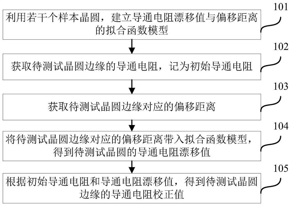
Method for obtaining on-resistance of wafer edge
A technology of on-resistance and wafer, applied in the direction of measuring resistance/reactance/impedance, circuits, electrical components, etc., can solve the problems of reducing the accuracy of test data, uneven negative pressure distribution, and different surface flatness, etc., to achieve correction Effects of on-resistance, improved stability, and reduced test error
- Summary
- Abstract
- Description
- Claims
- Application Information
AI Technical Summary
Problems solved by technology
Method used
Image

Examples
Embodiment Construction
[0042] The technical solutions in this application will be clearly and completely described below in conjunction with the accompanying drawings. Apparently, the described embodiments are part of the embodiments of this application, not all of them. Based on the embodiments in this application, all other embodiments obtained by persons of ordinary skill in the art without making creative efforts belong to the scope of protection of this application.
[0043] In the description of this application, it should be noted that the terms "center", "upper", "lower", "left", "right", "vertical", "horizontal", "inner", "outer" etc. The indicated orientation or positional relationship is based on the orientation or positional relationship shown in the drawings, and is only for the convenience of describing the present application and simplifying the description, rather than indicating or implying that the referred device or element must have a specific orientation, or in a specific orienta...
PUM
 Abstract
Description
Claims
Application Information
 - R&D Engineer
- R&D Manager
- IP Professional
- Industry Leading Data Capabilities
- Powerful AI technology
- Patent DNA Extraction
Browse by: Latest US Patents, China's latest patents, Technical Efficacy Thesaurus, Application Domain, Technology Topic, Popular Technical Reports.
© 2024 PatSnap. All rights reserved.Legal|Privacy policy|Modern Slavery Act Transparency Statement|Sitemap|About US| Contact US: help@patsnap.com