Device and method for compensating wedge-shaped error in wafer bonding

A wedge-shaped error and wafer bonding technology, which is applied in the fields of electrical components, semiconductor/solid-state device manufacturing, circuits, etc., can solve the bonding accuracy error of the upper and lower wafers, the non-parallel of the upper and lower wafers, wedge error, etc. problem, to achieve the effect of improving the accuracy

Active Publication Date: 2020-12-08
BEIJING U PRECISION TECH
View PDF5 Cites 2 Cited by
  • Summary
  • Abstract
  • Description
  • Claims
  • Application Information

AI Technical Summary

Problems solved by technology

[0004] When the wafers are aligned for pre-bonding, it often happens that the parallelism of t

Method used


Image

  • Device and method for compensating wedge-shaped error in wafer bonding
  • Device and method for compensating wedge-shaped error in wafer bonding
  • Device and method for compensating wedge-shaped error in wafer bonding

Examples


Example Embodiment

[0037] Example 1:

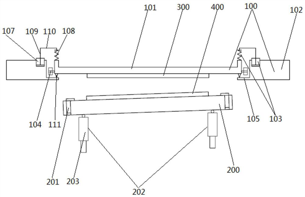
[0038] Embodiments of the present invention provide a device for compensating wedge errors in wafer bonding, such as figure 1 As shown, the device includes an upper stage 100 and a lower stage 200, wherein:

[0039] The lower bearing platform 200 is provided with a first adsorption device, the upper surface of the lower bearing platform 200 is provided with a gasket 201, the gasket 201 is connected with a gasket driving device, and the lower surface of the lower bearing platform 200 is provided with a lifting and angle adjusting device 202.

[0040] The upper bearing platform 100 includes an inner frame 101 and an outer frame 102, the edge area of ​​the inner frame 101 is located above the outer frame 102, and the inner frame 101 is floatingly connected to the outer frame 102 through the gravity balance device 103, so that the inner frame of the upper bearing platform floats on the upper bearing platform. On the outer frame of the stage, a plurality of cap...

Example Embodiment

[0054] Example 2:

[0055] An embodiment of the present invention provides a method for compensating wedge error in wafer bonding. The method is based on the device for compensating wedge error in wafer bonding described in Embodiment 1, and the method includes:

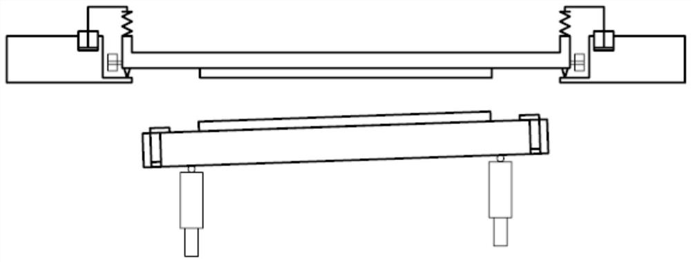
[0056] S1: The lower wafer is adsorbed on the upper surface of the lower carrier by the first adsorption device, and the upper wafer is adsorbed on the lower surface of the inner frame of the upper carrier by the second adsorption device, such as figure 2 shown.
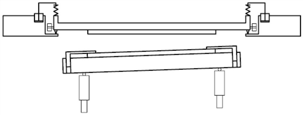
[0057] S2: The shims on the lower stage are advanced to the edge area of ​​the upper surface of the lower wafer by the shim drive device, such as image 3 shown.

[0058] S3: The gravity balance device performs gravity balance on the inner frame of the upper bearing platform, such as Figure 4 shown.

[0059] S4: The lower carrier is driven up by the lifting and angle adjustment device until it comes into contact with the upper wafer. The inner frame o...


PUM


Abstract

The invention discloses a device and a method for compensating a wedge-shaped error in wafer bonding, and belongs to the field of semiconductor wafer processing. The device comprises an upper bearingtable and a lower bearing table, a first adsorption device is arranged on the lower bearing table, a gasket is arranged on the upper surface of the lower bearing table, the gasket is connected with agasket driving device, and a lifting and angle adjusting device is arranged on the lower surface of the lower bearing table; the upper bearing table comprises an inner frame and an outer frame, the edge area of the inner frame is located above the outer frame, the inner frame is connected with the outer frame in a floating mode through a gravity balance device, a plurality of capacitance sensors are arranged on the edge area of the inner frame, and a second adsorption device is arranged on the inner frame. According to the invention, the wedge-shaped error between an upper wafer and a lower wafer is eliminated by adopting a wedge-shaped error compensation method, so that the two unparallel wafers are three-dimensionally parallel, and finally, the effect of improving the wafer bonding precision is achieved.

Description

technical field [0001] The invention relates to the field of semiconductor wafer processing, in particular to a device and method for compensating wedge errors in wafer bonding. Background technique [0002] A variety of semiconductor processes are involved in the IC manufacturing process. These processes require different equipment and methods. With the development of semiconductor processes from the micron level to the deep submicron and nanometer levels, there are precise work requirements for each subsystem of the IC manufacturing process. Higher and higher. [0003] As a key component of IC manufacturing equipment is the wafer alignment pre-bonding device, the accuracy and validity of this device will directly affect the success of wafer bonding. In the manufacturing process of the wafer alignment pre-bonding process, the first prerequisite to be met is to accurately align the two wafers, that is, after the surface treatment of the two wafers, the precise optical syste...

Claims


Application Information

Patent Timeline
IPC IPC(8): H01L21/18H01L21/66H01L21/68
CPCH01L21/187H01L22/12H01L22/26H01L21/68H01L22/32
Inventor 司伟杨光
Owner BEIJING U PRECISION TECH
Why Eureka
Try Eureka