Thin film transistor including oxide semiconductor layer

An oxide semiconductor and thin film transistor technology, which is applied in the manufacture of transistors, semiconductor devices, and semiconductor/solid-state devices, etc., can solve the problems of lower reliability, lower reliability, and threshold voltage deviation of display devices, and achieve high field effect mobility. , The effect of excellent light stress resistance

Pending Publication Date: 2020-12-15
KOBE STEEL LTD
View PDF3 Cites 0 Cited by
  • Summary
  • Abstract
  • Description
  • Claims
  • Application Information

AI Technical Summary

Problems solved by technology

[0006] In addition, when the liquid crystal panel is driven, or when a pixel is turned on by applying a negative bias to the gate electrode, etc., the light leaked from the liquid crystal cell is irradiated to the thin film transistor, but the light exerts stress on the thin film transistor. cause image unevenness or characteristic deterioration
When thin film transistors are actually used, if the switching characteristics change due to stress caused by light irradiation or voltage application, the reliability of the display device itself will decrease
[0007] In addition, in an organic EL display, light leakage from the light-emitting layer is also irradiated into the semiconductor layer, causing problems such as variations in threshold voltage and other values.
[0008] Such a shift in threshold voltage will lead to a decrease in the reliability of display devices such as liquid crystal displays and organic EL displays equipped with thin film transistors. Therefore, it is strongly desired to improve stress tolerance (that is, the amount of change before and after stress application is small)

Method used


Image

  • Thin film transistor including oxide semiconductor layer
  • Thin film transistor including oxide semiconductor layer
  • Thin film transistor including oxide semiconductor layer

Examples


Embodiment

[0086]

[0087] [Manufacturing of Thin Film Transistors]

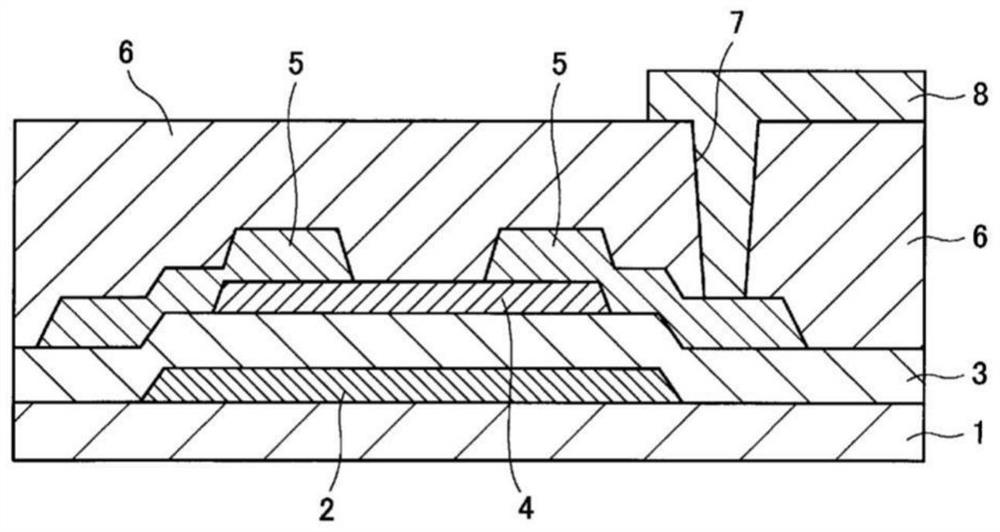
[0088] refer to figure 1 , the manufacturing method of the thin film transistor is shown below. On a glass substrate 1 (manufactured by Eagle, trade name Eagle 2000, 4 inches in diameter, 0.7 mm in thickness), a Mo film was formed to a thickness of 250 nm as a gate electrode. 2, and on it, use the plasma CVD method to form a film of silicon oxide (SiO x ) film as the gate insulating film 3.

[0089] Carrier gas: SiH 4 with N 2 Mixed gas of O

[0090] Film forming power density: 0.96W / cm 2

[0091] Film forming temperature: 320°C

[0092] Air pressure during film formation: 133Pa

[0093] Next, the oxide semiconductor layer 4 which is an In-Ga-Zn-Sn-O film described in Table 1 was formed with a film thickness of 40 nm under the following conditions.

[0094] (Oxide semiconductor layer formation)

[0095] Film formation method: DC (direct-current, DC) sputtering method

[0096] Device: CS200 manufactured by...

Embodiment 2

[0148] [The difference in post-annealing temperature vs. ΔV th Impact]

[0149] The stress tolerance (ΔV th @NBTIS) for comparison. The conditions of the stress application experiment were the same as described above.

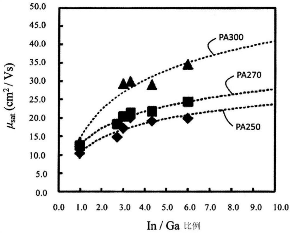
[0150] Figure 4 It shows the I of the ESL-TFT (thin film transistor) using the No. 3 oxide semiconductor layer when the post-annealing is performed at 250°C and when the post-annealing is performed at 300°C. d -V g characteristic chart. Furthermore, Figure 4 In , "PA250" indicates the case where the post-annealing was performed at 250°C, and "PA300" indicates the case where the post-annealing was performed at 300°C. According to the I d -V g characteristics to calculate the field-effect mobility (μ sat ), threshold voltage offset (V th ), subthreshold coefficient (subthreshold, SS) and on-current (I on ).

[0151] (in the case of post-annealing at 250°C)

[0152] Field Effect Mobility (μ sat ): 19.94cm 2 / Vs

[0153] Threshold Voltage Offset ...


PUM

PropertyMeasurementUnit
thicknessaaaaaaaaaa
thicknessaaaaaaaaaa
thicknessaaaaaaaaaa

Abstract

Provided is a thin film transistor provided with an oxide semiconductor layer thin film, wherein stress resistance, in particular light stress resistance, is improved while a high field effect mobility is maintained. A thin film transistor having, on a substrate, at least a gate electrode, a gate insulating film, an oxide semiconductor layer, source / drain electrodes, and at least one protective film, wherein: the metal elements constituting the oxide semiconductor layer include In, Ga, Zn, and Sn; and the proportion of each of the metal elements relative to the total of all metal elements (In+ Ga + Zn + Sn) is In: 30-45 atom% (inclusive); Ga: 5 atom% to less than 20 atom%; Zn: 30-60 atom% (inclusive); and Sn: 4.0 atom% to less than 9.0 atom%.

Description

technical field [0001] The present invention relates to a thin film transistor (Thin Film Transistor, TFT) containing an oxide semiconductor layer. More specifically, the present invention relates to a thin film transistor including an oxide semiconductor layer that is suitably used for a display device such as a liquid crystal display or an organic electroluminescence (EL) display. Background technique [0002] Amorphous (amorphous) oxide semiconductors have a higher carrier concentration than general-purpose amorphous silicon (a-Si), and are expected to be used in large-scale, high-resolution, and high-speed drives. in the next generation of displays. In addition, amorphous oxide semiconductors have a large optical band gap and can be formed at low temperatures, so they can be formed on resin substrates with low heat resistance, and are also expected to be used in light and transparent displays. . [0003] As the aforementioned amorphous oxide semiconductor, for example...

Claims


Application Information

Patent Timeline
Patent Type & Authority Applications(China)
IPC IPC(8): H01L29/786C23C14/08H01L21/336H01L21/363
CPCC23C14/08H01L29/7869H01L29/24H01L21/02565H01L21/02631
Inventor 越智元隆后藤裕史
Owner KOBE STEEL LTD
Why Eureka
Try Eureka