Level shift circuit

A level shift circuit and circuit technology, which is applied in the connection/interface layout of logic circuits, coupling/interfaces of logic circuits using field effect transistors, etc., can solve the problem that the DRV_OUT signal cannot be output normally, the gate oxide of the MOS tube is broken down, and it is not easy to flip. and other problems, to achieve the effect of novel technical solution, accurate power consumption value, accurate power consumption control and

Pending Publication Date: 2020-12-22
SUZHOU KAIWEITE SEMICON
View PDF0 Cites 0 Cited by
  • Summary
  • Abstract
  • Description
  • Claims
  • Application Information

AI Technical Summary

Problems solved by technology

[0005] This level shift structure uses narrow pulses to reduce the conduction time of N1 and N2, thereby reducing the power consumption on resistors R1 and R2, but the difficulty of this structure is that when N1 or N2 is turned on, R1 or The voltage at the lower end of R2 is directly pulled to 0V, otherwise it will cause the gate oxide breakdown of the MOS transistor of the RS latch behind, and at the same time, the power consumption on R1 or R2 is still too large, and it is not easy to control; if the lower end of R1 or R2 The voltage is pulled down too little, and the RS latch behind is not easy to flip, so the DRV_OUT signal cannot be output normally

Method used


Image

  • Level shift circuit
  • Level shift circuit
  • Level shift circuit

Examples


Embodiment 1

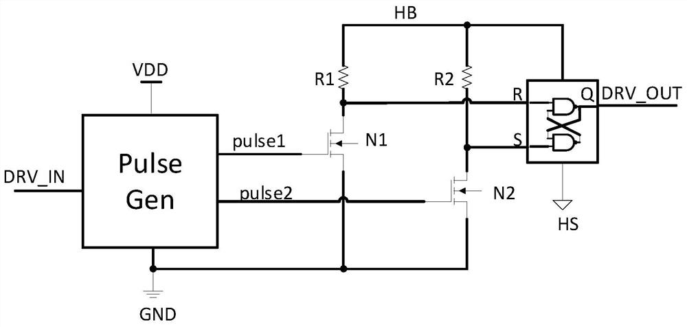
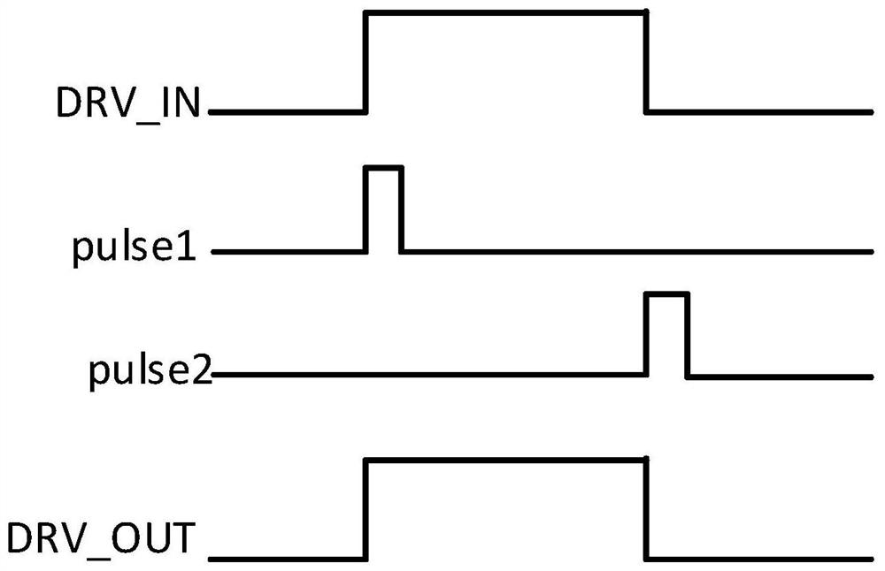
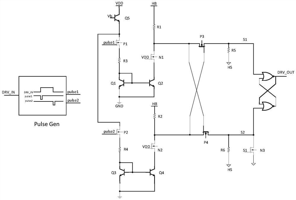
[0017] Embodiment 1: a level shift circuit, such as image 3 As shown, VDD is the chip power supply, usually 10-30V; GND is the chip ground; HB is the half-bridge high-side floating power supply, usually dozens of volts to hundreds of volts; HS is the half-bridge high-side floating ground; N1, N2 It is a MOS that withstands the high voltage of the half-bridge; R1 and R2 are two resistors that generate a voltage difference; Q1, Q2, Q3, and Q4 form two sets of current mirrors; Q5 is a current source that provides bias for the Q1 branch or Q3 branch respectively. The magnitude of the bias current is determined by the bias voltage Vb and the resistor R3 or R4; P1 and P2 are the switch tubes that control whether the two sets of current mirrors generate current, and are controlled by the pulse signal pulse1 and pulse2 respectively; P3 and P4 are the sampling The switch tube; R5, R6 resistors and N3 generate the initial state for the RS latch; the PulseGen module receives the DRV_IN ...


PUM


Abstract

The invention relates to a level shift circuit, which comprises a VDD as a chip power supply and a GND as a chip ground, the HB is a half-bridge high-side floating power supply; HS is half-bridge high-side floating ground; N1 and N2 are metal oxide semiconductors (MOS) for bearing half-bridge high voltage; wherein the resistor R1 and the resistor R2 are two resistors generating voltage difference;triodes Q1, Q2, Q3 and Q4 form two groups of current mirrors; the triode Q5 is a current source and provides bias current for the Q1 branch circuit or the Q3 branch circuit, and the magnitude of thebias current is determined by bias voltage Vb and a resistor R3 or R4; P1 and P2 are switching tubes for controlling whether the two groups of current mirrors generate current, and are respectively controlled by pulse signals pulse1 and pulse2; P3 and P4 are sampling switch tubes; R5, R6 and N3 are initial states generated by the RS latch; the PulseGen module receives a DRVIN signal and generatestwo paths of low and narrow pulse signals pulse1 and pulse2, the RS latch generates an output signal DRV_OUT, and the signal controls a subsequent driving circuit; the circuit is novel and concise, the circuit power consumption can be limited to be extremely low, and the power consumption value is accurate.

Description

technical field [0001] The invention relates to a level shift circuit and belongs to the technical field of power supply management. Background technique [0002] In the high-voltage half-bridge drive circuit, two drive signals need to be generated, one is high-side drive and the other is low-side drive, and the generation of high-side drive signals requires a special level shift circuit for voltage domain conversion. [0003] In the application, the high-voltage half-bridge application ranges from tens of volts to hundreds of volts, and the driver chip needs to integrate devices capable of withstanding this voltage to perform voltage domain conversion. Such as figure 1 Shown is the topological structure of the level conversion circuit in the prior art. VDD is the power supply voltage of the chip; GND is the chip ground; HB is the floating power supply voltage of the high voltage side of the half bridge; HS is the floating ground of the high voltage side of the half bridge...

Claims


Application Information

Patent Timeline
Patent Type & Authority Applications(China)
IPC IPC(8): H03K19/0185
CPCH03K19/0185
Inventor 涂才根张胜谭在超罗寅丁国华
Owner SUZHOU KAIWEITE SEMICON
Why Eureka
Try Eureka