SGT MOSFET device with bidirectional ESD protection capability

An ESD protection and capability technology, applied in the direction of electric solid-state devices, semiconductor devices, electrical components, etc., can solve the problems of large device area, process operability and controllability, etc., to reduce gate-drain capacitance and enhance ESD protection ability, effect of reducing deposition times

Pending Publication Date: 2021-01-01
VANGUARD SEMICON CORP
View PDF0 Cites 0 Cited by
  • Summary
  • Abstract
  • Description
  • Claims
  • Application Information

AI Technical Summary

Problems solved by technology

Anti-ESD design using multi-finger NMOSFET is an important method to improve the

Method used


Image

  • SGT MOSFET device with bidirectional ESD protection capability
  • SGT MOSFET device with bidirectional ESD protection capability

Examples


Embodiment Construction

[0024] Embodiments of the present invention are described below through specific examples, and those skilled in the art can easily understand other advantages and effects of the present invention from the content disclosed in this specification. The present invention can also be implemented or applied through other different specific implementation modes, and various modifications or changes can be made to the details in this specification based on different viewpoints and applications without departing from the spirit of the present invention.

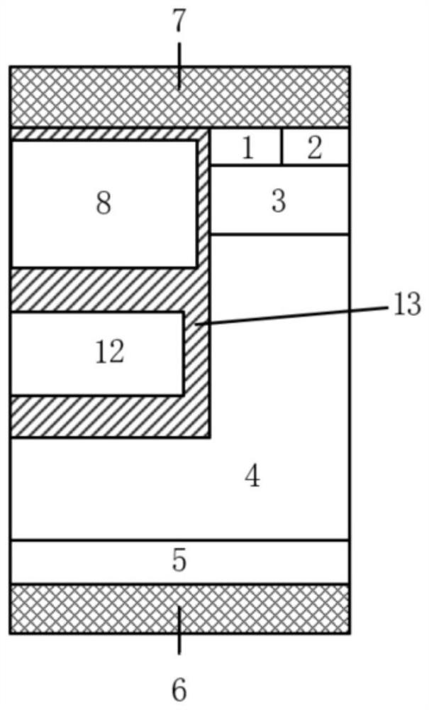
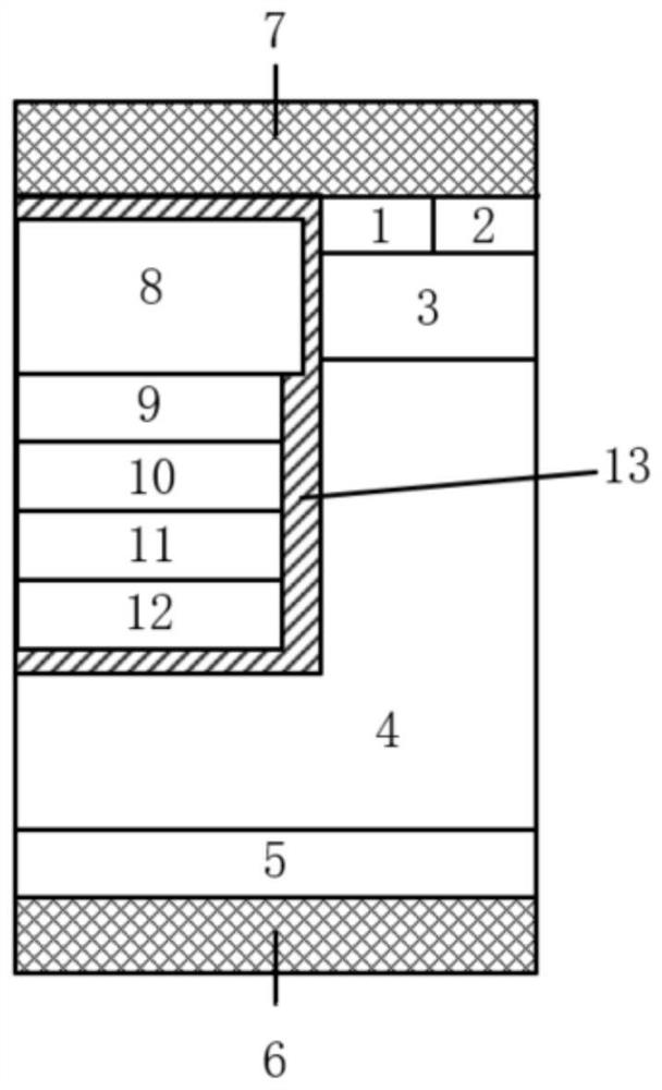
[0025] In order to realize the simultaneous improvement of both switching performance and ESD protection performance, the present invention proposes a SGTMOSFET device with bidirectional ESD protection capability based on the traditional SGTMOSFET structure and polysilicon multi-doped MOSFET structure, such as figure 2 shown. The main improvement of this structure is: changing the gate-dielectric layer-shielding gate structure in the...


PUM


Abstract

The invention discloses an SGT MOSFET device with bidirectional ESD protection capability, which comprises a cellular structure, and is characterized in that the cellular structure comprises drain metal, an N + substrate, an N-type drift region and source metal which are stacked in sequence from bottom to top; a trench gate structure is formed on one side of the upper surface of the N-type drift region, and the trench gate structure comprises an N + Poly gate, a P-type lightly doped region I, an N-type lightly doped region, a P-type lightly doped region II and an N-type source contact region which are sequentially arranged from top to bottom. On the basis of a traditional SGT MOSFET structure and a polycrystalline silicon multi-doped longitudinal MOSFET structure, the switching performanceand the ESD protection performance of the power MOS device are improved at the same time.

Description

technical field [0001] The invention relates to the technical field of power semiconductor devices, in particular to an SGT MOSFET device with bidirectional ESD protection capability. Background technique [0002] In the development of power devices, power MOSFETs have always played a very important role. The power MOSFET has experienced the development from horizontal to vertical, from planar gate to trench gate. Among them, the withstand voltage level, reliability and manufacturing process of vertical MOSFET are better than that of horizontal MOSFET. Trench gate changes the channel from horizontal to horizontal. The vertical completely eliminates the influence of the parasitic JFET resistance of the planar structure, greatly reduces the cell size while reducing the on-resistance, and greatly eliminates the disadvantages of the planar gate MOSFET, so that the trench vertical MOSFET has become the main development direction of the power MOSFET . [0003] Low-voltage trench...

Claims


Application Information

Patent Timeline
IPC IPC(8): H01L29/78H01L27/02
CPCH01L27/0255H01L29/7805H01L29/7813
Inventor 李泽宏赵一尚胡汶金林泳浩李伟聪
Owner VANGUARD SEMICON CORP
Why Eureka
Try Eureka