
Processing device

A technology for processing devices and holding surfaces, which is applied in the direction of static electricity, electrical components, and electrical solid devices, and can solve problems such as device quality degradation

Pending Publication Date: 2021-01-05
DISCO CORP
View PDF3 Cites 1 Cited by
  • Summary
  • Abstract
  • Description
  • Claims
  • Application Information

AI Technical Summary

Problems solved by technology

Therefore, static electricity may remain on the dicing tape, and the quality of the device may deteriorate.

Method used


Image

  • Processing device
  • Processing device
  • Processing device

Examples


Embodiment Construction

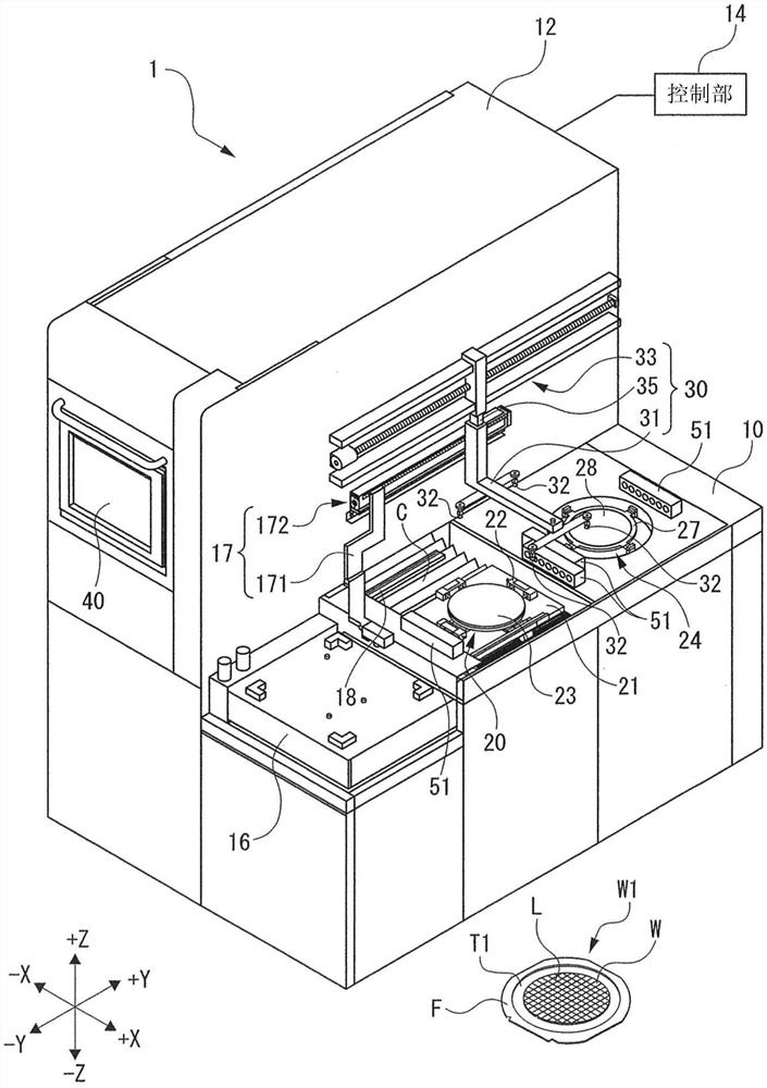
[0027] Such as figure 1 As shown, the cutting device 1 of this embodiment is an example of a processing device, and performs cutting processing on a wafer W as a workpiece.

[0028] The wafer W has a substantially circular shape, and grid-like planned dividing lines L are formed on the front surface. Various devices (not shown) are formed in each region divided by the planned division line L. As shown in FIG.

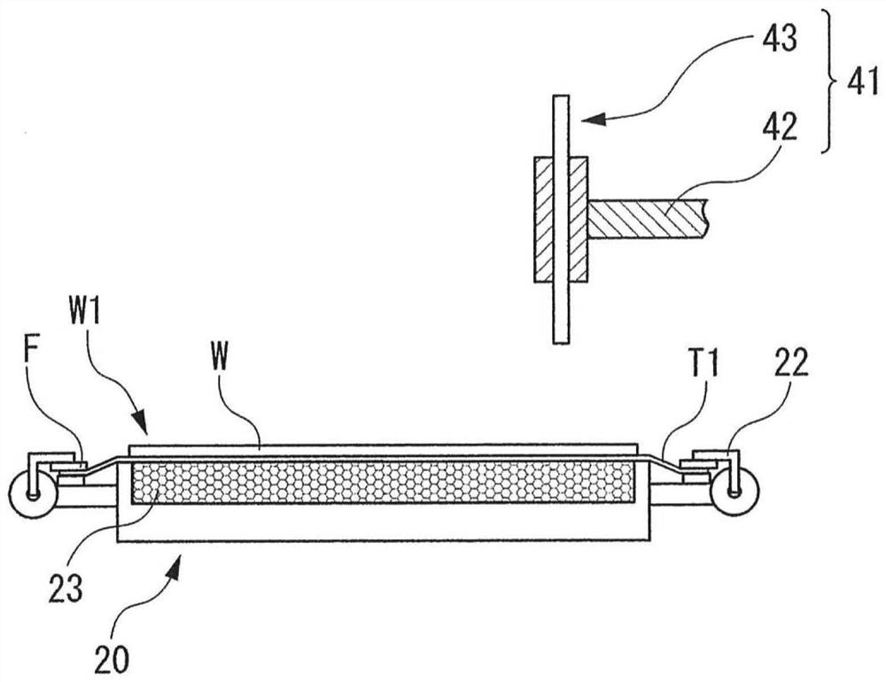
[0029] A dicing tape T1 is attached to the back surface of the wafer W. The ring frame F is attached to the outer periphery of the dicing tape T1. That is, the workpiece group W1 is formed by affixing and integrating the dicing tape T1 on the ring frame F and the wafer W disposed at the opening of the ring frame F.

[0030] In this manner, the wafer W is processed by the cutting device 1 in a state supported by the workpiece group W1 of the ring frame F via the dicing tape T1 . Furthermore, the workpiece group W1 is accommodated in a cassette not shown and carried i...


PUM


Abstract

A processing device is provided to remove the static electricity when the wafer is separated from the holding member. While gradually increasing the area of the part of the lower surface of the dicingtape (T1) which leaves the holding surface (23) of the chuck table (20), ionized air (A1) is blown to the part, thereby removing the static electricity of the dicing tape (T1). Therefore, it is possible to suppress the electrification of the dicing belt (T1) leaving the holding surface (23) of the chuck table (20), and remove the static electricity of the dicing belt (T1) while moving the work group (W1) out of the holding surface (23). Thus, the dicing tape (T1) leaving the holding surface (23) of the chuck table (20) is not easy to carry static electricity. Therefore, it is possible to suppress the degradation of the quality of the device formed on the wafer (W) of the work group (W1).

Description

technical field [0001] The invention relates to processing devices. Background technique [0002] In the chipping devices disclosed in Patent Document 1 and Patent Document 2, the wafer is chipped while being held by a holding member with a dicing tape attached to one surface thereof. [0003] In such a cutting device, after the cutting process, since the dicing tape attached to the wafer is charged with static electricity, the quality of the device formed on the wafer may deteriorate. Therefore, in order to remove static electricity charged on the dicing tape, ionized air is blown to the dicing tape. [0004] For example, in the cutting device disclosed in Patent Document 1, after the wafer on which the dicing tape is attached and held by the holding member is separated from the holding member by the carrying member, the air is changed so as to follow the rising wafer held by the carrying member. The direction of the jetting is such that the ionized air collides with the ...

Claims


Application Information

Patent Timeline
Patent Type & Authority Applications(China)
IPC IPC(8): H01L21/683H01L21/67H05F3/04H05F3/06
CPCH01L21/6835H01L21/67092H05F3/04H05F3/06H01L2221/68327H01L2221/68381H01L21/67132H01L21/6836
Inventor 新田秀次瓜田直功江角和也
Owner DISCO CORP
Learn More