Thin-membrane shaper, electrooptics device and electronic equipment

A thin film and particle technology, applied in the field of thin film forming devices, can solve problems such as disorder, molecular orientation disorder, and inability to obtain a stable ejection state, and achieve the effect of cost reduction

Inactive Publication Date: 2004-09-22
SEIKO EPSON CORP
View PDF3 Cites 8 Cited by
  • Summary
  • Abstract
  • Description
  • Claims
  • Application Information

AI Technical Summary

Problems solved by technology

[0012] However, in the conventional inkjet methods of Patent Documents 1 to 3, when foreign substances such as dirt and dust are mixed into the liquid crystal due to charging when the liquid crystal flows in the flow path, the display quality of the liquid crystal panel deteriorates. reduce
In addition, there is also the problem that a stable discharge state cannot be obtained due to the disorder of molecular orientation and the disorder of the meniscus of the liquid crystal ejection head.
[0013] In addition, when ions and the like are mixed into the liquid crystal, there will be a problem of poor display of the liquid crystal panel caused by ion conduction.

Method used


Image

  • Thin-membrane shaper, electrooptics device and electronic equipment
  • Thin-membrane shaper, electrooptics device and electronic equipment
  • Thin-membrane shaper, electrooptics device and electronic equipment

Examples


Embodiment Construction

[0054] Embodiments of the liquid crystal device for data writing according to the present invention will be described in detail below with reference to the accompanying drawings. Also, the present invention is not limited to this Example.

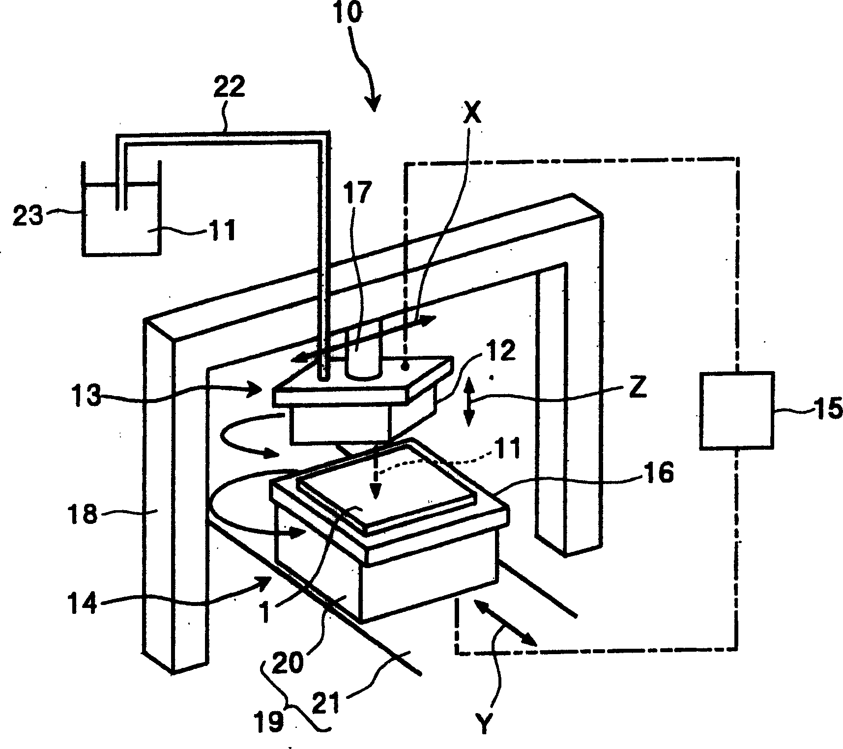
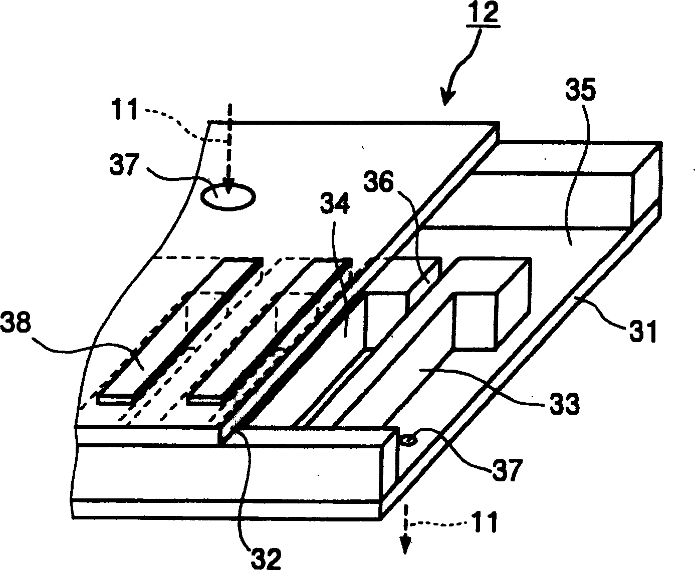
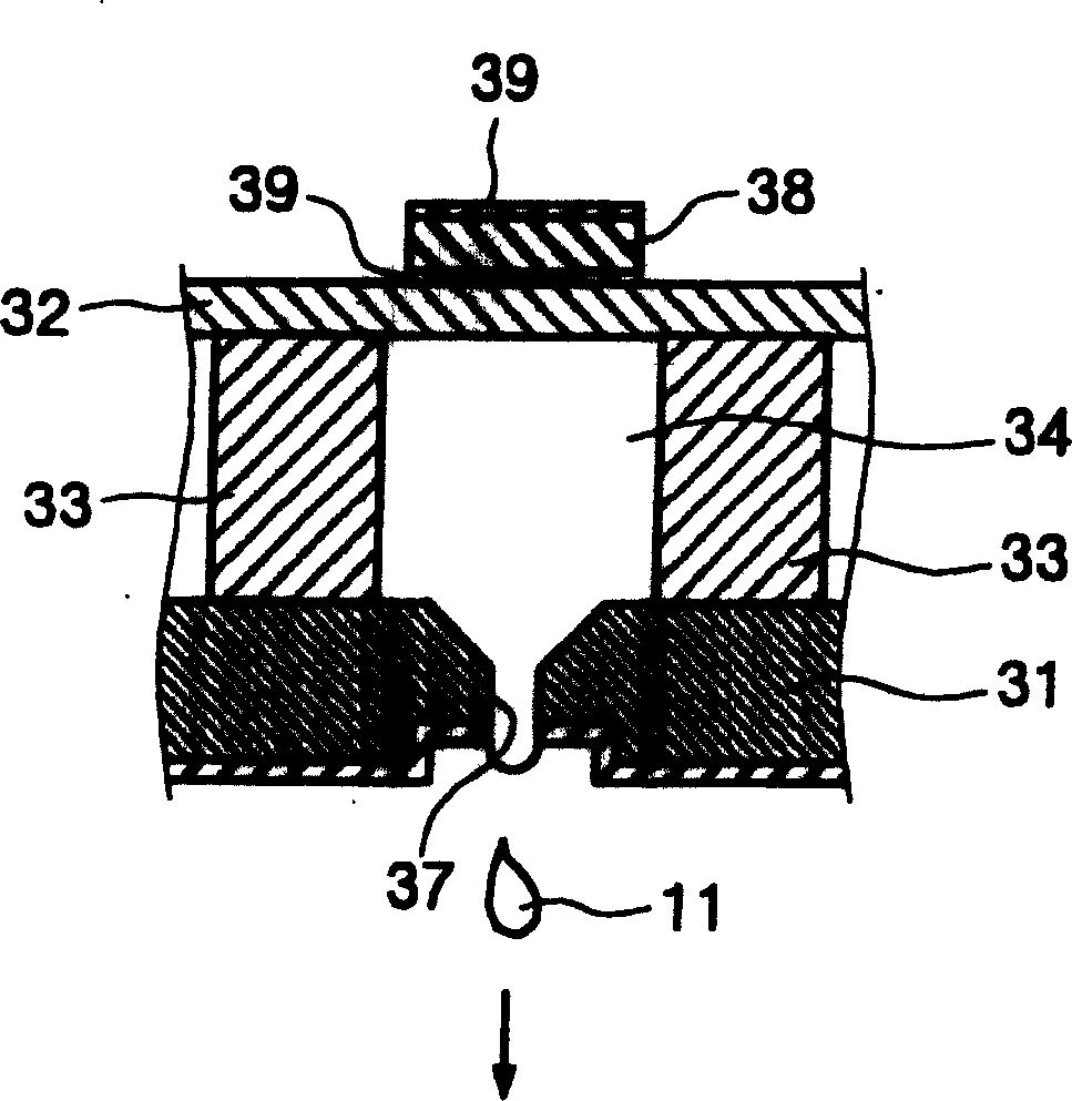
[0055] figure 1 It is a schematic diagram of the thin film forming apparatus of this invention. figure 2 and image 3 is a schematic diagram of a droplet ejection head. Figure 4 It is a configuration diagram of a liquid crystal panel.

[0056] First, refer to Figure 4 The configuration of the liquid crystal display panel as the electro-optical device of the present invention will be described. The liquid crystal display panel 100 of this embodiment has a first substrate 1 and a second substrate 4 facing each other, and liquid crystal display units 106 and 107 are respectively formed on the inner surfaces of the first substrate 1 and the second substrate 4 .

[0057] Specifically, as Figure 4 As shown, on the first substrate 1, a...


PUM


Abstract

There is provided a thin film fabrication apparatus that has a substrate stage, a droplet discharge head, a tank, and a tube. The substrate stage holds a substrate. The droplet discharge head is disposed above the substrate stage and discharges liquid crystal on the substrate. The tank contains the liquid crystal. The tube connects the tank and the discharge head to supply the liquid crystal from the tank to the discharge head. The tube and the tank are configured from antistatic material. The droplet discharge head is a piezojet type, and at least a part of the area in contact with the liquid crystal is configured from antistatic material.

Description

technical field [0001] The present invention relates to a thin film forming apparatus, and particularly to a thin film forming apparatus capable of improving the quality of a thin film and improving productivity. Background technique [0002] Generally, a liquid crystal device is manufactured by adding additional devices such as lighting devices such as backlights and liquid crystal driving ICs to a liquid crystal display panel having a structure in which liquid crystal is sealed between a pair of substrates. [0003] Additionally, if Figure 20 The liquid crystal display panel shown is generally manufactured by the following method. The first substrate 1 on which the first electrodes are formed and the second substrate 4 on which the second electrodes are formed are bonded to each other by using the sealing part 2. The gap between 1 and 4 is the cell gap, and the liquid crystal 3 is sealed. In addition, reference numeral 5 is a sealing portion that seals the injection port...

Claims


Application Information

Patent Timeline
Patent Type & Authority Applications(China)
IPC IPC(8): G02F1/13B05C5/00B41J2/16G02F1/1341H01L51/50H05B33/10
CPCG02F2001/13415G02F1/1341G02F1/13415F04B39/0044
Inventor 樱田和昭
Owner SEIKO EPSON CORP
Why Eureka
Try Eureka