Three-dimensional flash memory device supporting bulk erase operation and manufacturing method therefor

A flash memory device, three-dimensional technology, applied in the direction of semiconductor devices, electrical solid state devices, semiconductor/solid state device components, etc., can solve problems such as difficult to apply erasing operation, achieve the effect of improving integration and simplifying wiring process

Pending Publication Date: 2021-01-08
SAMSUNG ELECTRONICS CO LTD
View PDF0 Cites 0 Cited by
  • Summary
  • Abstract
  • Description
  • Claims
  • Application Information

AI Technical Summary

Problems solved by technology

[0015] However, in a three-dimensional flash memory device having a structure in which at least one intermediate wiring layer is arranged, since the channel layer in a string is divided into an upper channel layer and a lower channel layer due to at least one intermediate wiring layer, it is difficult to apply The erase operation of the bottom 200 block

Method used


Image

  • Three-dimensional flash memory device supporting bulk erase operation and manufacturing method therefor
  • Three-dimensional flash memory device supporting bulk erase operation and manufacturing method therefor
  • Three-dimensional flash memory device supporting bulk erase operation and manufacturing method therefor

Examples


Embodiment Construction

[0078] Hereinafter, embodiments of the present disclosure will be described in detail with reference to the accompanying drawings. However, the present disclosure is not limited to the embodiments described herein. Additionally, like components will be denoted by like reference numerals throughout the specification.

[0079] In addition, terms used herein are only for the purpose of appropriately describing the embodiments of the present disclosure, and may vary according to users, operator's intentions, custom in the art, and the like. Therefore, the terms used herein should be defined based on the descriptions throughout the specification.

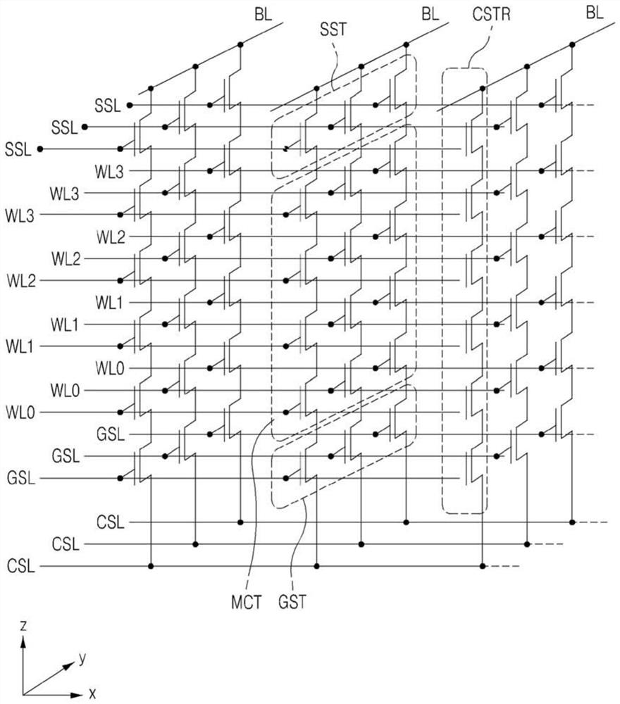
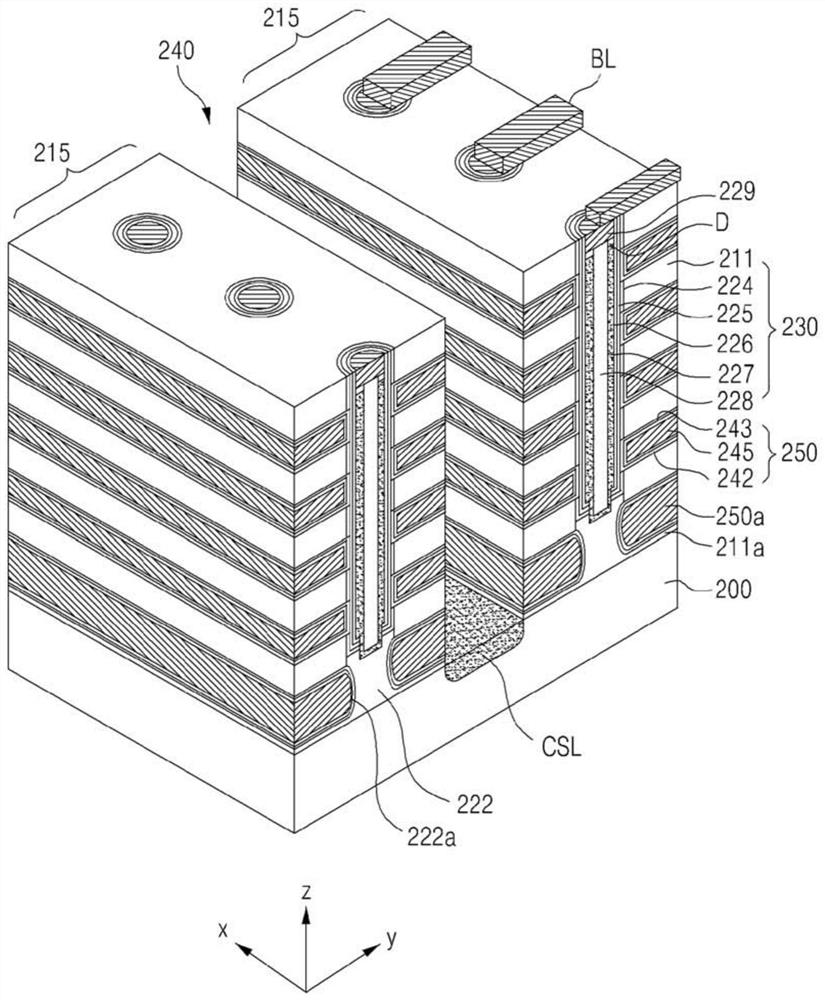
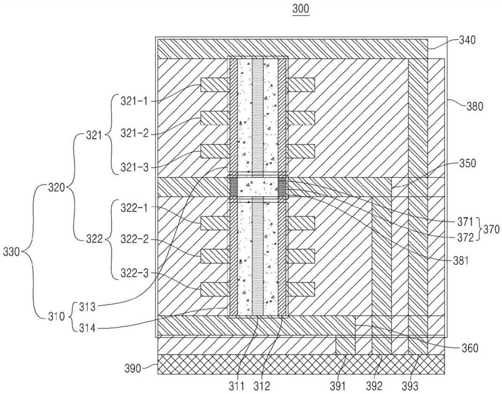
[0080] image 3 is a cross-sectional view illustrating a three-dimensional flash memory device supporting a bulk erase operation according to an embodiment of the present disclosure, Figure 4 show image 3 A bottom view of a region 380 of a three-dimensional flash memory device supporting a bulk erase operation, Figure 5 show im...


PUM


Abstract

Disclosed are a three-dimensional flash memory device supporting a bulk erase operation and a manufacturing method therefor. A three-dimensional flash memory device supporting a bulk erase operation,according to one embodiment, may comprise: a string including a channel layer configured to extend in one direction and a plurality of electrode layers vertically stacked with respect to the channel layer; an upper wiring layer disposed on an upper portion of the string; at least one intermediate wiring layer which penetrates through the channel layer in an intermediate area of the string and is disposed between the plurality of electrode layers; a lower wiring layer disposed on a lower portion of the string; and at least one connection part formed in the at least one intermediate wiring layerso as to connect at least two channel layers divided by the at least one intermediate wiring layer. A three-dimensional flash memory device including a buried intermediate wiring layer, according toanother embodiment, may comprise: a string including a channel layer configured to extend in one direction; a channel connection part for connecting, in an intermediate area of the string, an upper channel layer and a lower channel layer of the string to each other; an intermediate wiring layer which can be selectively used as any one from among a source electrode and a drain electrode for the string; and a wiring connection part for connecting the channel connection part and the intermediate wiring layer to each other while at least a part thereof is buried in the string.

Description

technical field [0001] The present disclosure relates to a three-dimensional flash memory device and a method for manufacturing the three-dimensional flash memory device, in particular to a three-dimensional flash memory device with a structure supporting a bulk erase operation. Background technique [0002] Flash memory devices are electrically erasable programmable read-only memory (EEPROM), and thus are commonly used in, for example, computers, digital cameras, MP3 players, game systems, memory sticks, and the like. Such a flash memory device controls input and output of data through Fowler-Nordheim tunneling (F-N tunneling) or hot electron injection. [0003] Specifically, refer to figure 1 , figure 1 An existing three-dimensional flash memory array is shown, and the existing three-dimensional flash memory array may include a common source line CSL, a bit line BL, and a plurality of cell strings CSTR between the common source line CSL and the bit line BL. [0004] Bit...

Claims


Application Information

Patent Timeline
Patent Type & Authority Applications(China)
IPC IPC(8): H01L27/11556H01L27/11524H01L27/11529
CPCG11C16/16G11C16/0483H10B43/35H10B43/27H01L23/5226H10B41/27
Inventor 宋润洽
Owner SAMSUNG ELECTRONICS CO LTD
Why Eureka
Try Eureka