Optical fingerprint identification module and forming method thereof

A fingerprint identification module and optical technology, applied in the field of image processing, can solve the problems of high optical fingerprint module, chip damage, unfavorable miniaturization of portable electronic devices, high integration, etc., to reduce reliability risks, avoid damage, Realize the effect of high integration

Pending Publication Date: 2021-01-12
GALAXYCORE SHANGHAI
View PDF0 Cites 0 Cited by
  • Summary
  • Abstract
  • Description
  • Claims
  • Application Information

AI Technical Summary

Problems solved by technology

In the prior art, the height of the side of the image sensor chip connected with the metal suspension wire is higher than the side of the printed circuit board 100 with the metal suspension wire, resulting in the overall height of the optical fingerprint module being too high, which is not conducive to the miniaturization of existing portable electronic devices , the trend of high integration, in addition, the chip 200 is directly bonded on the support plate 110, the drop, vibration, etc. in the actual use process may easily cause damage to the chip, and there is a high reliability risk

Method used


Image

  • Optical fingerprint identification module and forming method thereof
  • Optical fingerprint identification module and forming method thereof
  • Optical fingerprint identification module and forming method thereof

Examples


Embodiment Construction

[0042] In order to solve the above-mentioned problems in the prior art, the present invention provides an optical fingerprint recognition module and a forming method thereof.

[0043] In the following detailed description of the preferred embodiment, reference is made to the accompanying drawings which form a part hereof. The accompanying drawings show, by way of example, specific embodiments in which the invention can be practiced. The illustrated embodiments are not intended to be exhaustive of all embodiments in accordance with the invention. It is to be understood that other embodiments may be utilized and structural or logical changes may be made without departing from the scope of the present invention. Accordingly, the following detailed description is not limiting, and the scope of the invention is defined by the appended claims.

[0044] The present invention will be further elaborated below in conjunction with specific examples.

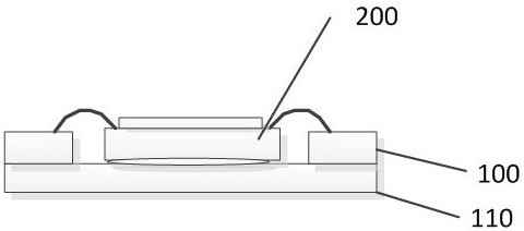
[0045] Please refer to Figure 2...


PUM


Abstract

The invention provides an optical fingerprint identification module and a forming method thereof. The optical fingerprint identification module comprises an image sensor chip and a printed circuit board, the image sensor chip is located in the hollow area of the printed circuit board in a suspended mode and is electrically connected to the printed circuit board only through a metal wire. The overall thickness of the optical fingerprint recognition module is smaller than the thickness of an existing module, the optical fingerprint recognition module can be suitable for a portable electronic device, the height of the module is reduced while the imaging effect is guaranteed, and high integration and high density of electronic devices are achieved.

Description

technical field [0001] The invention relates to the field of image processing, in particular to an optical fingerprint identification module and a forming method thereof. Background technique [0002] The current fingerprint identification schemes include optical technology, silicon technology (capacitive / radio frequency type), ultrasonic technology, etc. [0003] Optical technology The use of optical imaging equipment is based on the principle of total reflection of light (FTIR). The light hits the surface of the glass with fingerprints, and the reflected light is obtained by the image sensor. The amount of reflected light depends on the depth of the fingerprint ridges and valleys pressed on the surface of the glass, as well as the oil and moisture between the skin and the glass. After the light is shot to the center of the valley through the glass, it is totally reflected at the interface between the glass and the air, and the light is reflected to the image sensor, while...

Claims


Application Information

Patent Timeline
Patent Type & Authority Applications(China)
IPC IPC(8): G06K9/00
CPCG06V40/1318G06V40/1365
Inventor 赵立新侯欣楠
Owner GALAXYCORE SHANGHAI
Why Eureka
Try Eureka