Waveguide structure of annular resonant cavity with notch

A waveguide structure, resonant cavity technology, applied in the directions of light guide, optics, instruments, etc., can solve the problems of poor processing capability and integration, and achieve the effect of enhancing parallel processing capability and integration, and improving work efficiency

Pending Publication Date: 2021-01-22
GUANGDONG UNIV OF TECH
View PDF1 Cites 4 Cited by
  • Summary
  • Abstract
  • Description
  • Claims
  • Application Information

AI Technical Summary

Problems solved by technology

[0005] In order to overcome the problems of poor processing capability and integration of devices in the above-mentioned prior art, the present invention provides a waveguide structure with a notched annular resonant cavity, which produces a small-area, multi-channel, sharp and asymmetrical Fano Resonance, enhance the parallel processing capability and integration of optical devices

Method used


Image

  • Waveguide structure of annular resonant cavity with notch
  • Waveguide structure of annular resonant cavity with notch
  • Waveguide structure of annular resonant cavity with notch

Examples


Embodiment 1

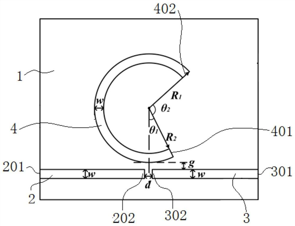
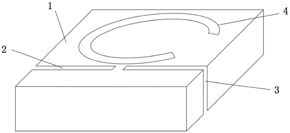
[0023] like Figure 1-2 Shown is an embodiment of a waveguide structure of a notched annular resonant cavity, including a substrate 1 and a first waveguide 2, a second waveguide 3 and a resonant cavity 4 disposed inside the substrate 1, the first waveguide 2 is from The first cavity extending from the side of the substrate 1 to the inside of the substrate 1; the second waveguide 3 extending from the side of the substrate 1 to the second cavity extending into the substrate 1, and the ends of the first cavity and the second cavity close to the side of the substrate 1 are both The openings are respectively the first openings 201 and 301, and the other ends are both closed ends, which are respectively the first closed end 202 and the second closed end 302; the resonant cavity 4 is a circular cavity with a gap, and the circular cavity The ends of are the third closed end 401 and the fourth closed end 402 respectively.

[0024] Wherein, the first waveguide 2 and the second waveguid...

Embodiment 2

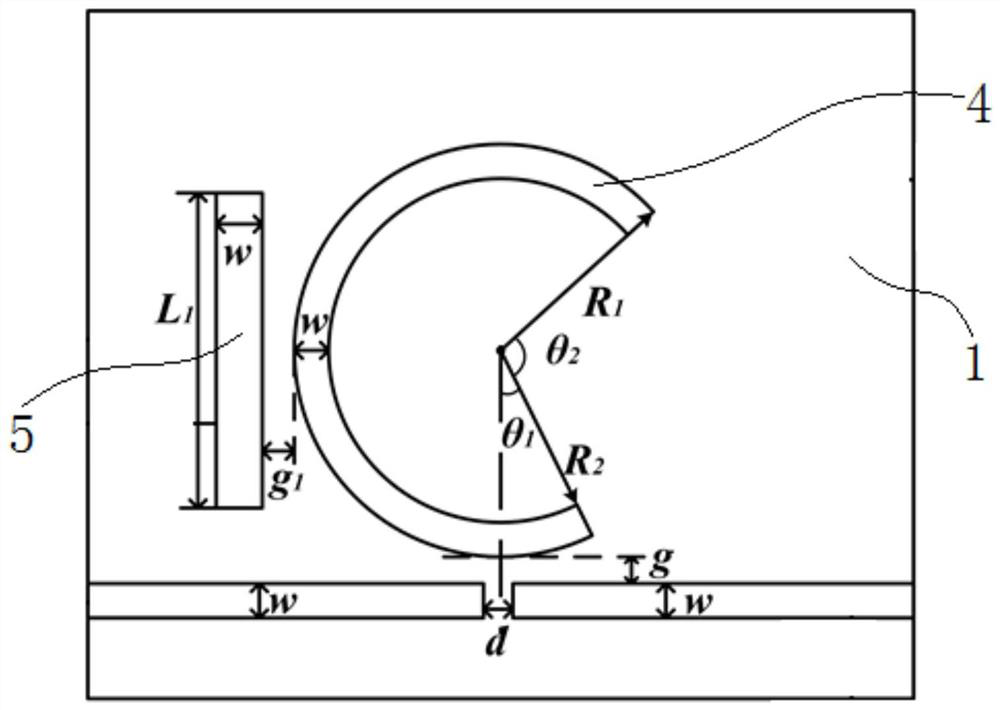
[0051] like image 3 Shown is another embodiment of the waveguide structure of a notched annular resonant cavity. The difference between this embodiment and the first embodiment is that a coupling resonant cavity 5 is provided on one side of the resonant cavity 4 . The dark mode provided by the coupled resonant cavity 5 interferes with the bright mode provided by the annular resonant cavity 4, so that more Fano resonance peaks can be formed.

[0052] The working principle or workflow of this embodiment: the parameters of the coupling resonant cavity 5 are set to:

[0053] L 1 =750nm, g 1 = 15nm. With such settings, new Fano resonance peaks with transmittances of 0.36, 0.36, and 0.23 can be formed at 109.8nm, 775nm, and 1183.4nm, respectively, and there are 12 Fano resonance channels in total. The wavelength and transmittance are shown in Table 6:

[0054]

[0055] Table 6 Wavelength and its corresponding transmittance

[0056] Of the Fano peaks that originally existed...


PUM

PropertyMeasurementUnit
transmittivityaaaaaaaaaa

Abstract

The invention relates to a waveguide structure of an annular resonant cavity with a notch. The waveguide structure comprises a substrate, a first waveguide, a second waveguide and the resonant cavity,wherein the first waveguide, the second waveguide and the resonant cavity are arranged in the substrate, and the first waveguide is a first cavity extending into the substrate from a side face of thesubstrate; the second waveguide is a second cavity extending into the substrate from the side face of the substrate; and the resonant cavity is an annular cavity with a notch. The resonant cavity isdesigned to be the annular cavity with the notch, so that small-area multi-channel Fano resonance is formed, the Fano resonance has the characteristics of sharpness and asymmetry, and each Fano resonance can output one function, so that the requirement of simultaneously processing data by multiple channels can be met, the parallel processing capacity and the integration level of an optical deviceare enhanced, therefore, the working efficiency of an optical circuit is improved.

Description

technical field [0001] The invention relates to the field of optical devices, more specifically, to a waveguide structure of a notched annular resonant cavity. Background technique [0002] Optical devices have been unable to realize highly integrated optical circuits due to the inherent diffraction limit of light. In recent years, surface plasmon polaritons (SPPs) generated by the coupling of light and metal surfaces have provided researchers with a new integrated optical circuit because of their ability to break through the diffraction limit and confine light in the sub-wavelength range. train of thought. Metal-medium-metal (MIM) waveguide structures based on SPPs have attracted people's attention and have been widely used in the sub-wavelength range. Different from the Lorentz resonance, the Fano resonance produced by the interference between the bright mode (continuous state) and the dark mode (separated state) of the MIM waveguide structure has an asymmetric and sharp...

Claims


Application Information

Patent Timeline
Patent Type & Authority Applications(China)
IPC IPC(8): G02B6/122G02B6/125
CPCG02B6/122G02B6/125
Inventor 温坤华吴楚华李铮峰方翼鸿郭子聪沈丽红
Owner GUANGDONG UNIV OF TECH
Why Eureka
Try Eureka