Eureka AIR delivers breakthrough ideas for toughest innovation challenges, trusted by R&D personnel around the world.

Manufacturing method of semiconductor device, and semiconductor device

A manufacturing method and semiconductor technology, applied in semiconductor devices, electric solid state devices, electrical components, etc., can solve problems such as crosstalk, and achieve the effects of reducing interference, improving effectiveness and reliability

Inactive Publication Date: 2021-01-22
YANGTZE MEMORY TECH CO LTD
View PDF5 Cites 4 Cited by
  • Summary
  • Abstract
  • Description
  • Claims
  • Application Information

AI Technical Summary

Problems solved by technology

However, this creates crosstalk issues

Method used


Image

  • Manufacturing method of semiconductor device, and semiconductor device
  • Manufacturing method of semiconductor device, and semiconductor device
  • Manufacturing method of semiconductor device, and semiconductor device

Examples


Embodiment Construction

[0062] The following will clearly and completely describe the technical solutions in the embodiments of the present invention with reference to the drawings in the embodiments of the present invention. Apparently, the described embodiments are only some of the embodiments of the present invention, but not all of them. Based on the embodiments of the present invention, all other embodiments obtained by those skilled in the art without making creative efforts belong to the protection scope of the present invention.

[0063]It will be understood that although the terms first, second, etc. may be used herein to describe various components, these components should not be limited by these terms. These terms are used to distinguish one component from another. For example, a first component could be termed a second component, and, similarly, a second component could be termed a first component, without departing from the scope of the present invention.

[0064] It will be understood...


PUM


Abstract

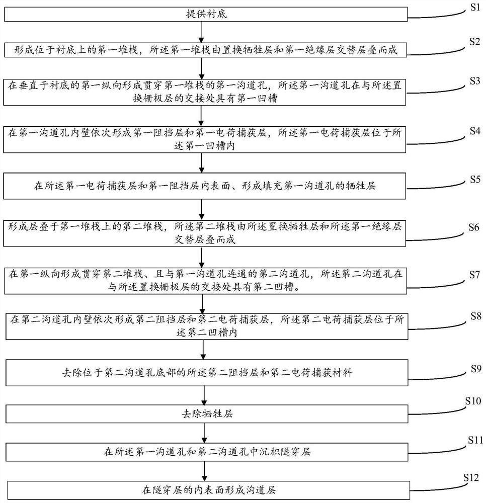
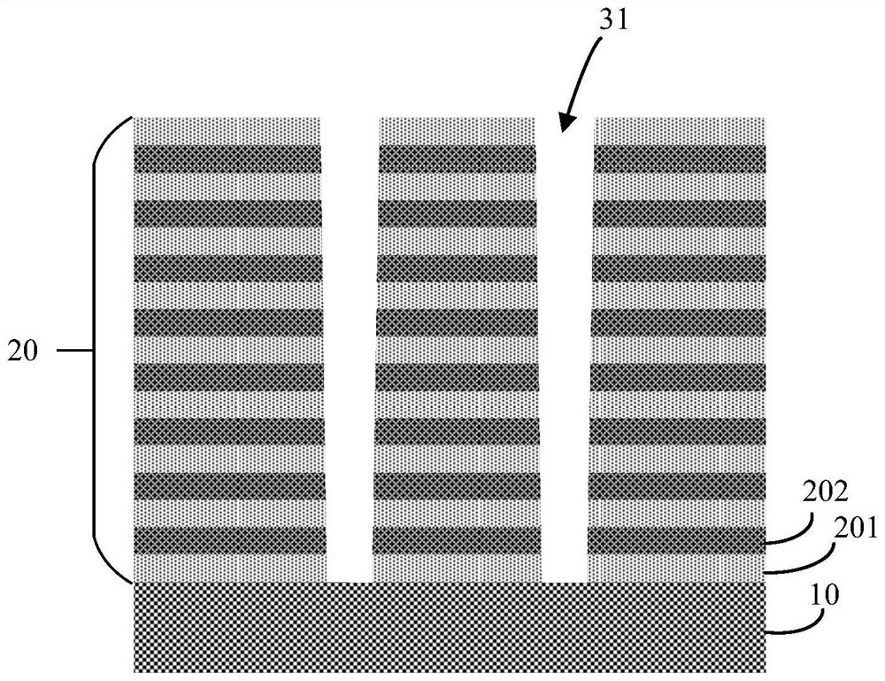
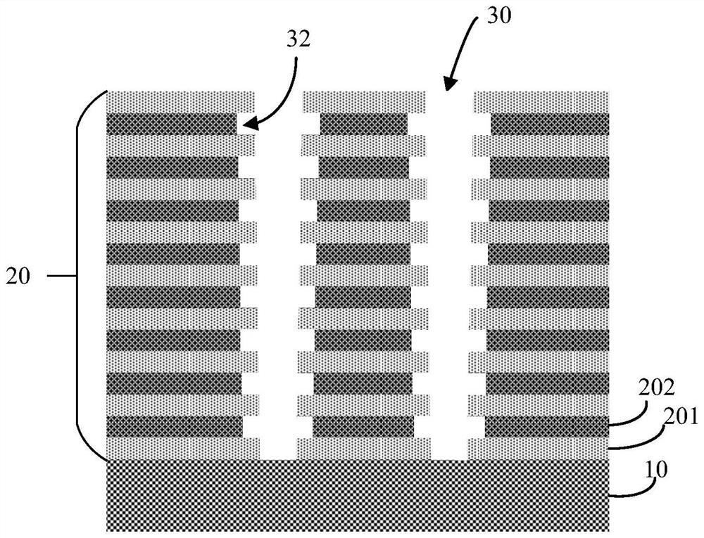
The invention discloses a manufacturing methodfor a semiconductor device, and a semiconductor device. The method comprises the following steps: firstly forming a channel hole with a groove, then forming a blocking layer in the channel hole, and then forming charge trapping layers on the inner surface of the blocking layer in the groove, wherein the first charge trapping layes are separated in a first longitudinal direction. The separated charge trapping layers can effectively prevent stored charges from diffusing among a plurality of storage units, so interference among the storage units is reduced, and the effectiveness and reliability of reading and writing of the semiconductor device can be further improved.

Description

technical field [0001] The present invention generally relates to the field of semiconductors, and in particular, relates to a method for manufacturing a semiconductor device and the semiconductor device. Background technique [0002] NAND storage devices are non-volatile storage products with low power consumption, light weight and good performance, and are widely used in electronic products. The planar NAND device is close to the limit of actual expansion. In order to further increase the storage capacity and reduce the storage cost per bit, 3D NAND memory is proposed. In the 3D NAND memory structure, a stacked memory structure is realized by vertically stacking multiple layers of data storage units. [0003] To increase the storage density of 3D NAND flash memory by vertically stacking a larger number of memory cells, as the aspect ratio of the channel hole increases, it will cause manufacturing problems in the process, such as the non-uniformity of the channel hole and ...

Claims


Application Information

Patent Timeline
IPC IPC(8): H01L27/1157H01L27/11582
CPCH10B43/35H10B43/27
Inventor 高庭庭薛磊刘小欣耿万波
Owner YANGTZE MEMORY TECH CO LTD
Why Eureka
Eureka Blog
Learn More