A connection structure and method between a db small board and a pcb board

A PCB board and connection method technology, which is applied in the field of connection structure between DB small board and PCB board, can solve the problems of high defect rate, leakage and outflow of defective products, and achieve good tinning effect, avoid defective products, and reliable connection

Active Publication Date: 2021-12-03
ZHEJIANG KAIYAO LIGHTING
View PDF3 Cites 0 Cited by
  • Summary
  • Abstract
  • Description
  • Claims
  • Application Information

AI Technical Summary

Problems solved by technology

Now the commonly used DB small board, the gold finger copper foil on it is directly spread to the edge of the board, the through hole on the gold finger is inserted into the PCB board and exposed, the gold finger of the DB small board after the furnace is not tinned, and the defect rate reaches 100%. To solve this problem, it is necessary to add workers after the furnace to add tin 100%. However, due to the high defect rate, some defective products still leak and flow out

Method used


Image

  • A connection structure and method between a db small board and a pcb board
  • A connection structure and method between a db small board and a pcb board
  • A connection structure and method between a db small board and a pcb board

Examples


Embodiment

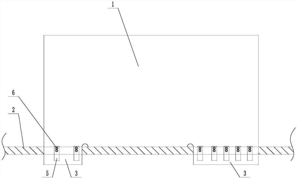
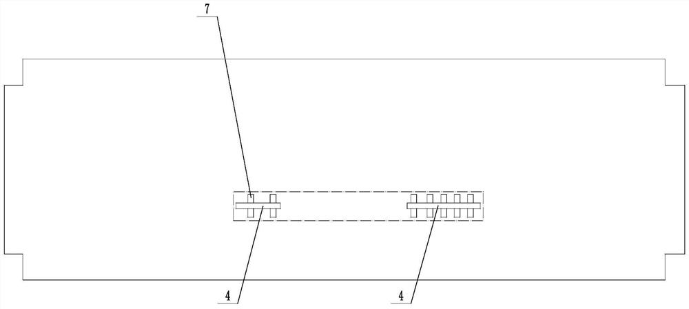
[0025] Example: DB one kind of a small PCB board connected to the plate structure (see attached figure 1 Attachment figure 2 ), A small plate comprising a DB 1, PCB board 2, the edges of the small plate is provided with DB extending outwardly projecting connecting portions 3, PCB board and the connecting portion is provided with a corresponding slot adapted 4, a plurality of spaced connecting portions 5 cheat pad, finger pad provided with a through-hole 6 at one end, the other end is provided with Goldfinger pad spacing between the edge portions of the connector, PCB pads to the slot edge and a correspondence set Goldfinger there are a number of lug 7, a connection portion inserted in the slot, finger pads expose the lower surface of the PCB through hole hidden in the slot, finger pads and the corresponding welding lug. DB embodiment a lower edge of the small plate of the present embodiment is provided with right and left connection portions each position, provided two gold finger...


PUM


Abstract

The invention discloses a connection structure and method of a DB small board and a PCB board, aiming to solve the problems that the gold fingers of the DB small board cannot be tinned and the rate of defective products is high after the DB small board and the PCB board are connected to a furnace. The invention includes a DB small board and a PCB board. The edge of the DB small board is provided with an outwardly extending and protruding connecting portion, and the PCB board is provided with slots corresponding to the connecting portion. There is a through hole at one end of the gold finger pad, and there is a gap between the other end of the gold finger pad and the edge of the connection part. There are several solder pieces corresponding to the edge of the slot on the PCB board and the gold finger pad. The bottom is inserted into the slot, the gold finger pad is exposed on the bottom surface of the PCB, the through hole is hidden in the slot, and the gold finger pad and the solder piece are soldered correspondingly. The connection between the DB small board and the PCB board is reliable, and the gold fingers of the DB small board are full of tin after the furnace, which avoids defective products.

Description

Technical field [0001] The present invention relates to a circuit board connection structure, and more particularly, it relates to a structure and method for a small plate DB is connected to the PCB. Background technique [0002] In recent years, LED lighting drive its energy-saving and environmental protection, beautiful and delicate features are gradually replace the original traditional fluorescent tubes, and gradually occupied most of the home lighting and intelligent lighting direction. Wherein due to the rapid increase in the smart function, and the driving range in size than before, not only No increase but at a decreasing trend. The market demand, so the product derived by inserting a small plate DB, to solve the conventional patch can be affixed to the bottom surface and the front surface of the drive layout. DB now commonly used in small plates, finger directly on a copper foil plated board edge, after insertion the bare PCB board Goldfinger above through hole, the DB i...

Claims


Application Information

Patent Timeline
Patent Type & Authority Patents(China)
IPC IPC(8): H05K1/14H05K1/11
CPCH05K1/116H05K1/141H05K2201/044H05K2201/09372
Inventor 张科侍昌山
Owner ZHEJIANG KAIYAO LIGHTING
Why Eureka
Try Eureka