Semiconductor wafer integral cleaning equipment

A technology for cleaning equipment and semiconductors, which is applied in semiconductor/solid-state device manufacturing, electrical components, circuits, etc., and can solve problems such as long working hours, heavy physical exertion of workers, and wafer damage

Inactive Publication Date: 2021-02-02
太仓治誓机械设备科技有限公司
View PDF0 Cites 5 Cited by
  • Summary
  • Abstract
  • Description
  • Claims
  • Application Information

AI Technical Summary

Problems solved by technology

[0002] As we all know, semiconductor wafers can be processed into circuit components, and their main component is silicon. During the processing and production of semiconductor wafers, it is necessary to clean up the debris left by the surface processing, so as to make the surface of the wafer clean and prevent the debris from affecting the subsequent processing. The existing cleaning method is mainly to manually wash the double sides of the wafer slowly through water flow. When using this method, it is necessary to continuously flip each group of wafers so that the debris is washed away from the wafer. The cleaning method It is more cumbersome, the working time is longer, the cleaning efficiency is low, the physical strength of the workers is greater, and the stability of the workers' hands is poor, the hardness of the wafer is small, and the wafer is easily damaged when the wafer is manually turned over to clean it. Stubborn debris tends to remain on the wafer

Method used


Image

  • Semiconductor wafer integral cleaning equipment
  • Semiconductor wafer integral cleaning equipment
  • Semiconductor wafer integral cleaning equipment

Examples


Embodiment Construction

[0021] The specific implementation manners of the present invention will be further described in detail below in conjunction with the accompanying drawings and embodiments. The following examples are used to illustrate the present invention, but are not intended to limit the scope of the present invention.

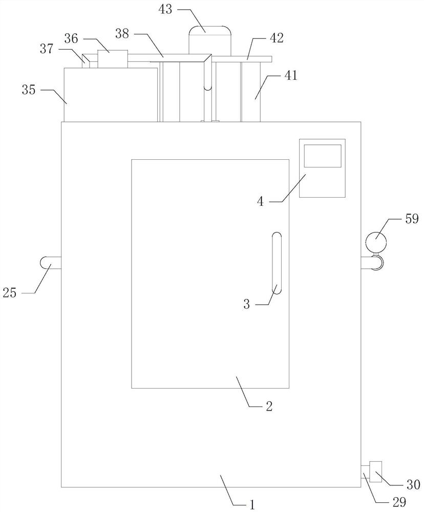
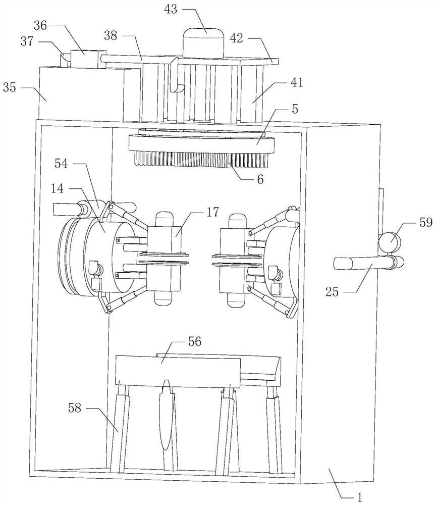
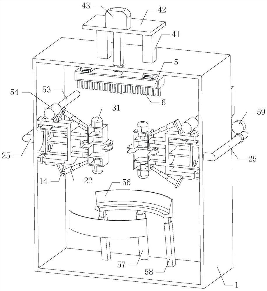
[0022] Such as Figure 1 to Figure 7 As shown, a kind of overall semiconductor wafer cleaning equipment of the present invention, when it is working, the operating mode of the turning device is that the central control box 4 controls to open the power device, and the power device drives the worm wheel 15 on the turning device to rotate, and the worm wheel 15 drives The rotating bucket 14 rotates, and the rotating bucket 14 drives the annular chute 13 to slide on the annular guide rail 12. When the second ventilation hole 11 is turned over to the upper side of the second ventilation hole 11, the second ventilation hole 11 on the original upper side is turned over to the po...


PUM


Abstract

The invention relates to the technical field of mechanical equipment, in particular to semiconductor wafer integral cleaning equipment, which can effectively save the physical strength and time duringmanual cleaning, simplify the cleaning mode and improve the working efficiency by performing automatic cleaning treatment on a wafer, and is high in stability during equipment operation. The stability of the wafer overturning and cleaning work is improved, the wafer can be protected conveniently, damage to the wafer is reduced, the wafer is washed and cleaned, the cleaning effect can be effectively improved, and the practicability and reliability are improved; the equipment comprises a cleaning bin, a bin door, a handle, a central control box and a water guide disc, the front side of the cleaning bin communicates with a bin opening, the bin door is hinged to the bin opening, the handle is installed on the bin door, the central control box is installed on the cleaning bin, the water guidedisc is located on the upper side in the cleaning bin, and a first cavity is formed in the water guide disc; and a water injection device and a rotary pushing device are arranged at the top of the cleaning bin.

Description

technical field [0001] The invention relates to the technical field of mechanical equipment, in particular to a semiconductor wafer overall cleaning equipment. Background technique [0002] As we all know, semiconductor wafers can be processed into circuit components, and their main component is silicon. During the processing and production of semiconductor wafers, it is necessary to clean up the debris left on the surface, so as to make the surface of the wafer clean and prevent the debris from affecting subsequent processing. The existing cleaning method is mainly to manually wash the double sides of the wafer slowly through water flow. When using this method, it is necessary to continuously flip each group of wafers so that the debris is washed away from the wafer. The cleaning method It is more cumbersome, the working time is longer, the cleaning efficiency is low, the physical strength of the workers is greater, and the stability of the workers' hands is poor, the hardn...

Claims


Application Information

Patent Timeline
IPC IPC(8): H01L21/67
CPCH01L21/67057
Inventor 吴禹凡高洪庆
Owner 太仓治誓机械设备科技有限公司
Why Eureka
Try Eureka