

Semiconductor memory and method for forming the same
A memory and semiconductor technology, applied in semiconductor/solid-state device manufacturing, semiconductor devices, semiconductor/solid-state device components, etc., can solve problems such as increasing the fineness of patterns and increasing the integration of two-dimensional semiconductor memory devices
- Summary
- Abstract
- Description
- Claims
- Application Information
AI Technical Summary
Problems solved by technology
Method used
Image

Examples
Embodiment Construction
[0024] Example embodiments of the inventive concepts will now be described more fully with reference to the accompanying drawings, in which example embodiments are shown.
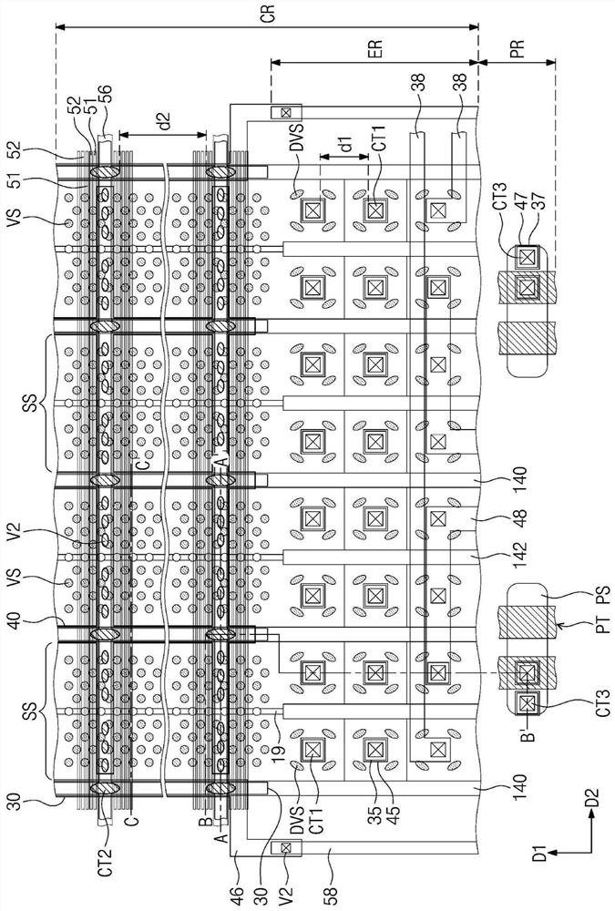
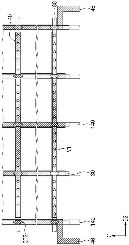
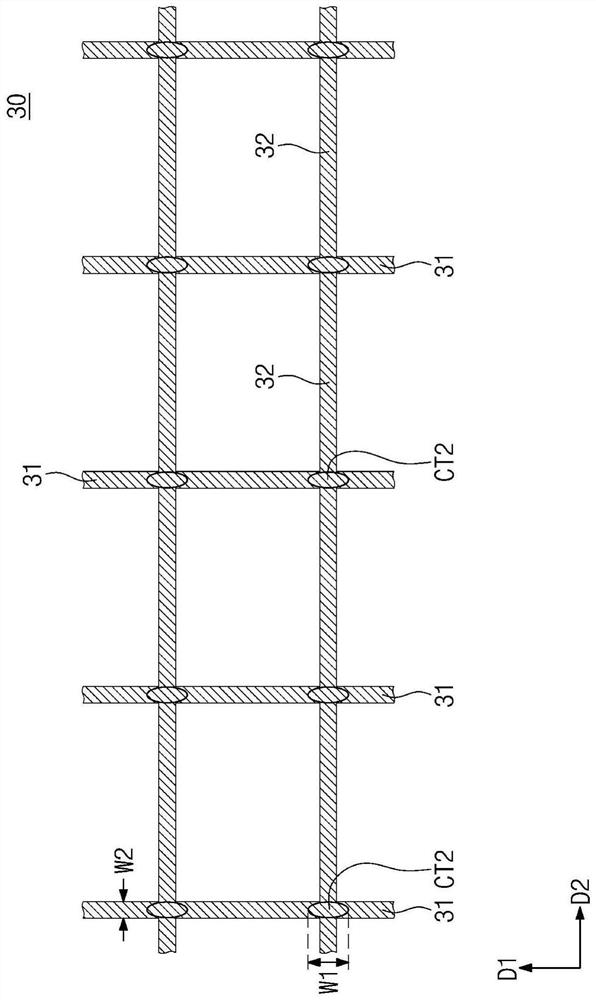
[0025] figure 1 is a plan view illustrating a semiconductor memory device according to an embodiment of the inventive concept. figure 2 is a plan view showing the first interconnection structure and the second interconnection structure. image 3 is a plan view of the first interconnect structure. Figure 4 is a plan view of the second interconnect structure. Figure 5A , Figure 5B and Figure 5C respectively along the figure 1 Cross-sectional views taken along line A-A', line BB' and line CC' of .
[0026] refer to Figure 1 to Figure 4 , Figure 5A , Figure 5B and Figure 5C , a semiconductor memory device including a cell array region CR and a peripheral circuit region PR can be provided. As an example, the semiconductor memory device may be a flash memory device. The cell array region CR m...
PUM
 Abstract
Description
Claims
Application Information