Integrated circuit layout initialization and optimization method and device, storage medium and equipment

A technology of integrated circuits and optimization methods, applied in electrical digital data processing, computer-aided design, instruments, etc., can solve problems affecting the position of data sending and receiving nodes, affecting the layout of chips or modules, and not having enough space for wiring, etc. To achieve the effect of scientific and reasonable layout, optimized layout and increased distance in the early stage

Pending Publication Date: 2021-02-09
BEIJING BAIRUI INTERNET TECH CO LTD
View PDF0 Cites 3 Cited by
  • Summary
  • Abstract
  • Description
  • Claims
  • Application Information

AI Technical Summary

Problems solved by technology

[0002] The main technical points that need to be considered in the initial layout of integrated circuit design include: input and output issues, no matter what chip or module ultimately needs to communicate with the outside of the chip or module, then it is necessary to specify the location of these communication ports, these communication ports The selection of the location of the chip or module will often significantly affect the internal layout of the chip or module; the density problem, when a large amount of logic is concentrated in a small physical area, the area may have a problem of excessive density, and the problem of excessive density is usually easy to cause The problem of insufficient power supply or insufficient space for wiring; the problem of rational use of space, because the size and shape of various devices are different, putting them in the layout is like a puzzle, how to make better use of space is a problem; timing convergence Problem, the layout will greatly affect the position of the data sending and receiving nodes, thus greatly affecting the timing, how to make the timing easier to converge is also an important issue; and the problem of low power consumption, in the design of modern low-power integrated circuits usually It is necessary to divide a chip into multiple different power supply areas, use different power supply voltages or cut off the power supply of some areas when needed, so as to achieve the purpose of reducing power consumption, but this brings great challenges to the layout of the chip. challenge

Method used


Image

  • Integrated circuit layout initialization and optimization method and device, storage medium and equipment
  • Integrated circuit layout initialization and optimization method and device, storage medium and equipment
  • Integrated circuit layout initialization and optimization method and device, storage medium and equipment

Examples


Embodiment Construction

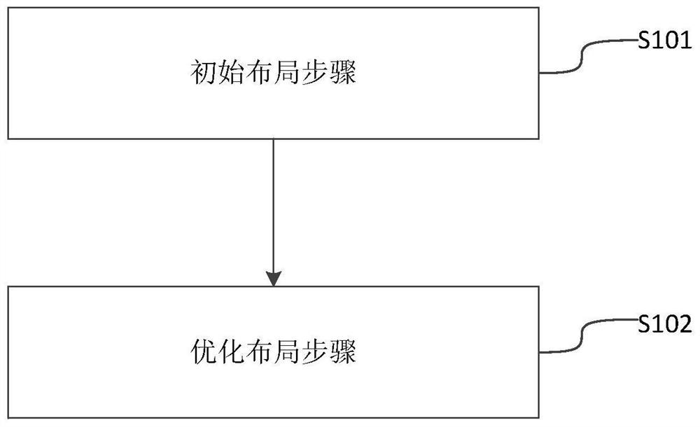
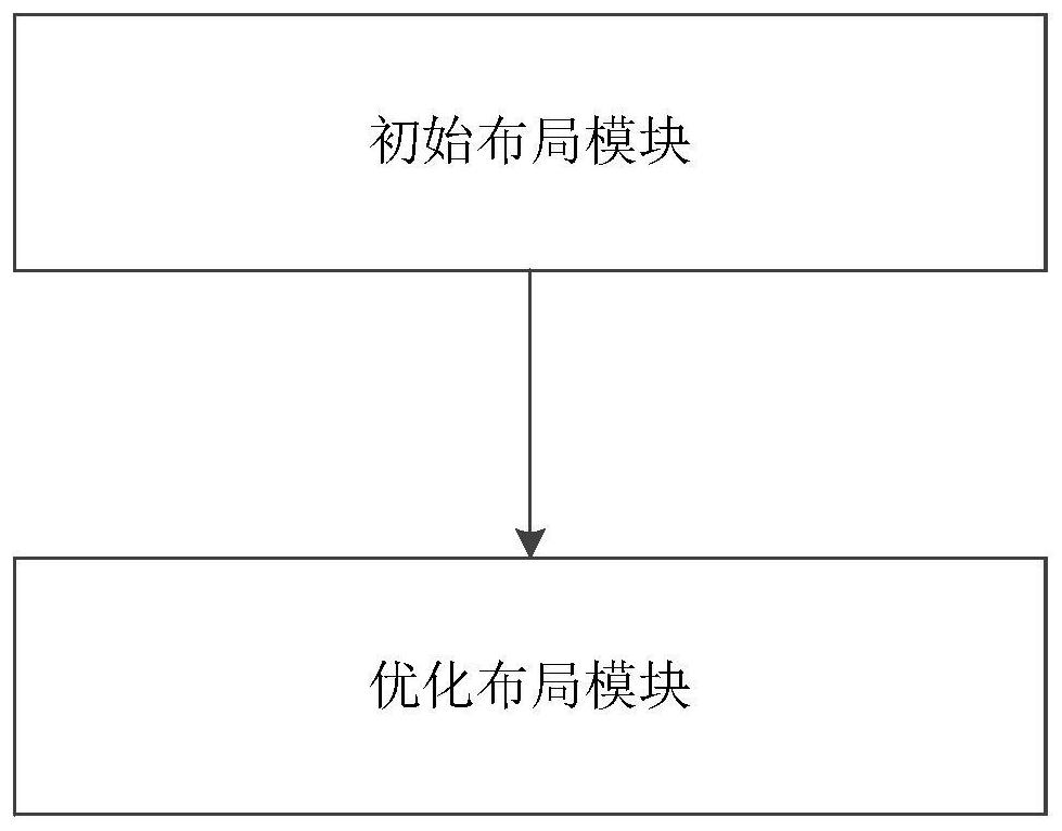
[0011] The preferred embodiments of the present invention will be described in detail below in conjunction with the accompanying drawings, so that the advantages and features of the present invention can be more easily understood by those skilled in the art, so as to define the protection scope of the present invention more clearly.

[0012] It should be noted that in this article, relational terms such as first and second are only used to distinguish one entity or operation from another entity or operation, and do not necessarily require or imply that there is a relationship between these entities or operations. There is no such actual relationship or order between them. Furthermore, the term "comprises", "comprises" or any other variation thereof is intended to cover a non-exclusive inclusion such that a process, method, article, or apparatus comprising a set of elements includes not only those elements, but also includes elements not expressly listed. other elements of or a...


PUM


Abstract

The invention discloses an integrated circuit layout initialization and optimization method and device and a storage medium, and belongs to the field of integrated circuit design. The method comprisesthe following steps: analyzing and placing a plurality of IP modules of an integrated circuit in a blank physical layout area of the integrated circuit by using a data flow analysis tool, and dividing IP position grids with the same area on the blank physical layout area at the periphery of each IP module in the plurality of IP modules, and placing an external function module in the area, exceptthe IP position grids, of the blank physical layout area by utilizing a standard unit arrangement too; and performing simulation adjustment on the positions of at least two of the plurality of IP modules, and performing actual position adjustment on the at least two of the plurality of IP modules according to the change of the time sequence snapshot state space size before and after the simulationadjustment. The application of the method is separated from qualitative analysis, the relative positions of the IP modules are analyzed through a time sequence, and the weight is increased, so that the positions of the IP modules are conveniently exchanged, the layout optimization is realized, and the early-stage layout is more scientific and reasonable.

Description

technical field [0001] The present application relates to the technical field of integrated circuit design, in particular to an integrated circuit layout initialization and optimization method, device, storage medium and equipment. Background technique [0002] The main technical points that need to be considered in the initial layout of integrated circuit design include: input and output issues, no matter what chip or module ultimately needs to communicate with the outside of the chip or module, then it is necessary to specify the location of these communication ports, these communication ports The selection of the location of the chip or module will often significantly affect the internal layout of the chip or module; the density problem, when a large amount of logic is concentrated in a small physical area, the area may have a problem of excessive density, and the problem of excessive density is usually easy to cause The problem of insufficient power supply or insufficien...

Claims


Application Information

Patent Timeline
Patent Type & Authority Applications(China)
IPC IPC(8): G06F30/392G06F30/394G06F30/398G06F30/3312
CPCG06F30/3312G06F30/392G06F30/394G06F30/398
Inventor 葛颖峰朱勇徐祎喆
Owner BEIJING BAIRUI INTERNET TECH CO LTD
Why Eureka
Try Eureka