LCP packaging substrate, manufacturing method and multi-chip system-in-package structure
A technology for packaging substrates and chips, which is used in semiconductor/solid-state device manufacturing, semiconductor/solid-state device components, semiconductor devices, etc., to achieve the effects of good compatibility, low moisture absorption and water permeability, oxygen permeability, and high integration density
- Summary
- Abstract
- Description
- Claims
- Application Information
AI Technical Summary
Problems solved by technology
Method used
Image

Examples
Embodiment 1
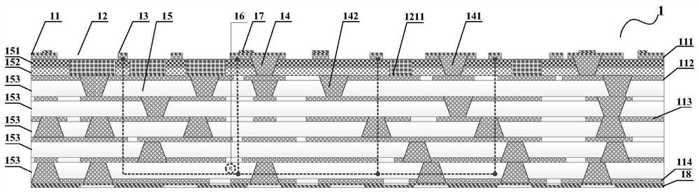
[0069] Such as figure 1 As shown, a kind of LCP packaging substrate of the present embodiment comprises:
[0070] n layers of patterned metal circuit layers distributed from the surface to the bottom surface, the first layer of patterned metal circuit layers, the second layer of patterned metal circuit layers, ..., the nth layer of patterned metal circuit layers; the nth layer of patterned The metal circuit layer is provided with a structure for soldering BGA solder balls;
[0071] n-1 layers of insulating dielectric layer between adjacent patterned metal circuit layers; insulating dielectric layer between the first layer of patterned metal circuit layer and the second layer of patterned metal circuit layer, bonded by LCP substrate and LCP The melting point of the LCP adhesive film is lower than that of the LCP substrate; the insulating medium layer between the second patterned metal circuit layer and the nth patterned metal circuit layer is a non-LCP material substrate, and ...
Embodiment 2
[0089] Such as Figure 4 As shown, the present embodiment provides a method for manufacturing the LCP packaging substrate 1 as described in Embodiment 1, comprising the following steps:
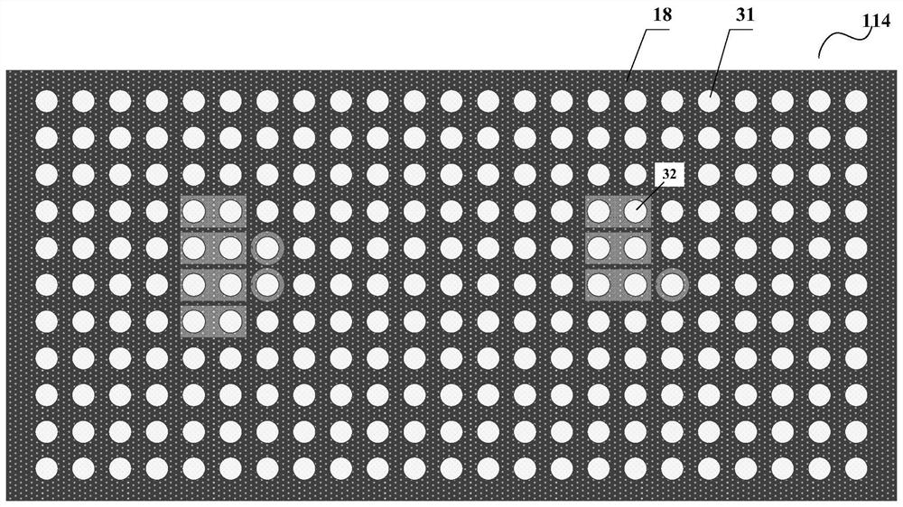
[0090] S1, such as Figure 5a As shown, the non-LCP material multilayer interconnection multilayer substrate is manufactured by HDI lamination process; the non-LCP material multilayer interconnection multilayer substrate includes the second patterned metal circuit layer 112 to the n-1th layer patterned metal circuit Layer 113, the underlying large-area metal copper layer for making the nth patterned metal circuit layer 114, the insulating dielectric layer 15 and a plurality of blind holes 14 between adjacent patterned metal circuit layers; the non-LCP material is optional The insulating dielectric layer in the layer-interconnection multilayer substrate is a non-LCP material substrate 153; wherein, the blind holes here are the second type of blind holes, and the depth-to-diameter ratio of the...
Embodiment 3
[0100] Such as Figure 6 As shown, based on the LCP packaging substrate described in Embodiment 1-2, this embodiment provides a multi-chip system-in-package structure 61, including: the LCP packaging substrate 1 described in Embodiment 1-2, and BGA solder balls 2. Chip 3, metal frame 5 and metal cover 6;
[0101] The BGA solder balls 2 are soldered to the bottom surface of the LCP packaging substrate 1, and serve as the external secondary cascade I / O interface of the multi-chip system-in-package structure 61;
[0102] Metal partitions 51 are distributed in the metal enclosure 5; the metal enclosure 5 and the metal partitions 51 are welded to the upper surface of the LCP packaging substrate 1, and the metal cover 6 is welded to the metal enclosure 5 and the metal partitions 51, between the LCP packaging substrate 1 and the metal cover plate 6, a plurality of cavity structures 7 with airtight sealing performance and electromagnetic shielding performance are formed through the m...
PUM
 Abstract
Description
Claims
Application Information
 - R&D
- Intellectual Property
- Life Sciences
- Materials
- Tech Scout
- Unparalleled Data Quality
- Higher Quality Content
- 60% Fewer Hallucinations
Browse by: Latest US Patents, China's latest patents, Technical Efficacy Thesaurus, Application Domain, Technology Topic, Popular Technical Reports.
© 2025 PatSnap. All rights reserved.Legal|Privacy policy|Modern Slavery Act Transparency Statement|Sitemap|About US| Contact US: help@patsnap.com