Wafer test classification method and system

A technology of wafer testing and classification methods, applied in semiconductor/solid-state device testing/measurement, electrical components, semiconductor/solid-state device manufacturing, etc., can solve the problem of uncontrollable FT yield rate in mass production of high-performance product specifications and inability to effectively process performance Requires production and testing process chip products, high production and testing costs, etc.

Active Publication Date: 2021-02-19
HYGON INFORMATION TECH CO LTD
View PDF8 Cites 20 Cited by
  • Summary
  • Abstract
  • Description
  • Claims
  • Application Information

AI Technical Summary

Problems solved by technology

[0004] In view of this, the embodiment of the present invention provides a wafer test classification method and system, which is used to solve the problem that the existing technology cannot effectively handle the classification of chip produc...

Method used


Image

  • Wafer test classification method and system
  • Wafer test classification method and system
  • Wafer test classification method and system

Examples


Embodiment Construction

[0112] Embodiments of the present invention will be described in detail below in conjunction with the accompanying drawings.

[0113] It should be clear that the described embodiments are only some of the embodiments of the present invention, not all of them. Based on the embodiments of the present invention, all other embodiments obtained by persons of ordinary skill in the art without creative efforts fall within the protection scope of the present invention.

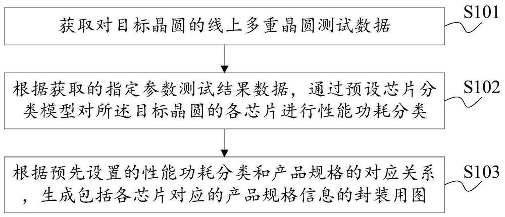
[0114] figure 1 It is a schematic flowchart of Embodiment 1 of a wafer test classification method provided by an embodiment of the present invention. see figure 1 , the method includes the following steps before the encapsulation step:

[0115] Step S101, obtaining online multi-wafer test data for the target wafer;

[0116] Wherein, the test data includes the specified parameter test result data of the target wafer under different temperature and voltage test conditions;

[0117] In this embodiment, the test and ...


PUM


Abstract

The embodiment of the invention discloses a wafer test classification method and system, belongs to the technical field of chips, and the method comprises the steps: obtaining the online multi-wafer test data of a target wafer before a packaging step, wherein the test data comprises specified parameter test result data of the target wafer under different temperature and voltage test conditions; performing performance power consumption classification on each chip of the target wafer through a preset chip classification model according to the acquired specified parameter test result data; and generating a packaging graph including product specification information corresponding to each chip according to a preset corresponding relationship between the performance power consumption classification and the product specification. According to the invention, offline chip performance analysis and classification can be carried out according to wafer test parameters, thereby achieving the purposes of improving the performance level of a final device, meeting the requirements of product specifications with different performance and power consumption, and improving the productivity of actual products.

Description

technical field [0001] The invention belongs to the field of chip technology, and in particular relates to a wafer test classification method and system. Background technique [0002] After the wafer manufacturing is completed, wafer testing is required, that is, before the wafer is sent to the packaging factory, qualified chips need to be identified through wafer testing. Wafer testing is one of the main statistical methods for chip yield. The current technical solution in the industry is: the wafer test classification and data processing are mainly completed by the test program during the chip test process, and the subsequent packaging is directly cut and packaged according to the wafer test classification results. [0003] It can be seen that the classification and packaging of chips in the prior art directly depend on the contents and test results of the wafer test program. However, the testing process of the existing technical solution is complicated and the cost is hi...

Claims


Application Information

Patent Timeline
IPC IPC(8): H01L21/66H01L21/67
CPCH01L22/20H01L22/10H01L21/67271Y02P90/30
Inventor 滕为荣江华陆毅张珩
Owner HYGON INFORMATION TECH CO LTD
Why Eureka
Try Eureka