Automatic film pasting equipment for surface of semiconductor wafer

A film laminating equipment and semiconductor technology, which is applied in semiconductor/solid-state device manufacturing, electrical components, circuits, etc., can solve problems such as wafer damage, bubble residue, and poor bubble extrusion effect

Inactive Publication Date: 2021-02-23
太仓联科工业设计有限公司
View PDF0 Cites 8 Cited by
  • Summary
  • Abstract
  • Description
  • Claims
  • Application Information

AI Technical Summary

Problems solved by technology

[0002] As we all know, the wafer is the basic raw material for making semiconductor electrical components. It is mainly cut from silicon rods. When the wafer is processed and produced, it usually needs to be treated with a film on its surface to protect the surface of the wafer. The existing wafer The method of round film sticking is mainly to manually stick the film on the surface of the wafer, and then use the roller to squeeze out the air bubbles between the film and the surface of the wafer, so that the vacuum state between the film and the surface of the wafer is achieved, and the film is automatically It is adsorbed on the surface of the wafer, and then the excess film on the wafer is manually cut off to achieve the purpose of wafer film attachment. However, when this method is used, the effect of the roller on the air bubbles between the film and the wafer is poor, and it is easy to This results in tiny air bubbles remaining, resulting in a poor film attachment effect. Due to the low hardness of the wafer, it is easy to cause damage to the wafer when the roller is squeezed. At the same time, this film attachment method requires manual operation, the film attachment speed is slow, and the work efficiency is low. Need to consume excess manpower

Method used


Image

  • Automatic film pasting equipment for surface of semiconductor wafer
  • Automatic film pasting equipment for surface of semiconductor wafer
  • Automatic film pasting equipment for surface of semiconductor wafer

Examples


Embodiment Construction

[0022] The specific implementation manners of the present invention will be further described in detail below in conjunction with the accompanying drawings and embodiments. The following examples are used to illustrate the present invention, but are not intended to limit the scope of the present invention.

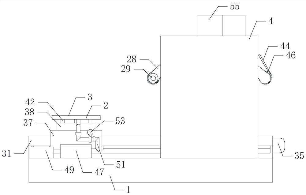
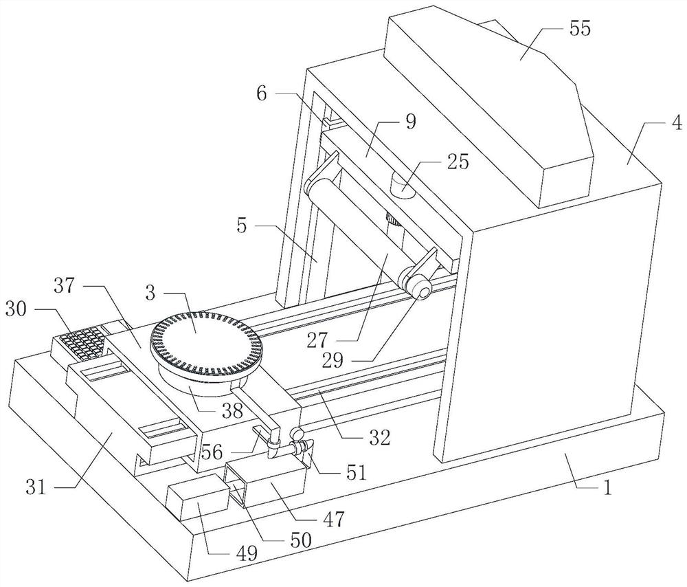
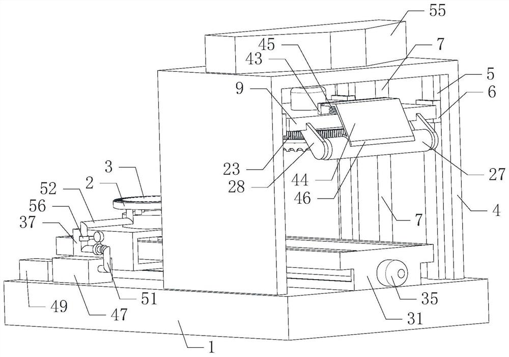
[0023] Such as Figure 1 to Figure 8As shown, the semiconductor wafer surface automatic film sticking equipment of the present invention, when it is working, the protruding end of the winding film on the right winding roller 27 is wound on the left winding roller 27, so that the bottom of the pressure ring 21 is covered with film, the wafer is placed on the rubber pad 3, the position of the wafer is aligned with the position of the circular adsorption chamber 2, the central control box 30 controls the opening of the suction device, and the suction device sucks the air in the circular adsorption chamber 2 Negative pressure is formed inside the circular adsorption chamber 2...


PUM


Abstract

The invention relates to the technical field of wafer processing equipment, in particular to automatic film pasting equipment for the surface of a semiconductor wafer, which can effectively save the physical strength and time during manual film pasting operation and improve the film pasting work efficiency by performing automatic film pasting treatment on a semiconductor wafer; meanwhile, the bubble removal effect between a film and the wafer is improved, the bubble residuals are avoided, and the effect is effectively improved. According to the wafer protection device, the stress intensity ofthe wafer is monitored in real time, so that the wafer can be conveniently protected, the wafer is prevented from being extruded and damaged, and the practicability and reliability are improved; the equipment comprises a base, a circular adsorption bin, a rubber pad and a first arc-shaped plate; a transverse pushing device is arranged at the top of the base, a pressure detection device is arrangedon the left side of the transverse pushing device, the circular adsorption bin is installed on the pressure detection device, and the rubber pad is installed at the top of the circular adsorption bin; multiple groups of conical holes are uniformly formed in the outer side of the top of the rubber pad; and the bottoms of the multiple sets of conical holes communicate with the interior of the circular adsorption bin.

Description

technical field [0001] The invention relates to the technical field of wafer processing equipment, in particular to automatic film sticking equipment on the surface of semiconductor wafers. Background technique [0002] As we all know, the wafer is the basic raw material for making semiconductor electrical components. It is mainly cut from silicon rods. When the wafer is processed and produced, it usually needs to be treated with a film on its surface to protect the surface of the wafer. The existing wafer The method of round film sticking is mainly to manually stick the film on the surface of the wafer, and then use the roller to squeeze out the air bubbles between the film and the surface of the wafer, so that the vacuum state between the film and the surface of the wafer is achieved, and the film is automatically It is adsorbed on the surface of the wafer, and then the excess film on the wafer is manually cut off to achieve the purpose of wafer film attachment. However, w...

Claims


Application Information

Patent Timeline
Patent Type & Authority Applications(China)
IPC IPC(8): H01L21/67
CPCH01L21/67126
Inventor 吴禹凡高洪庆
Owner 太仓联科工业设计有限公司
Why Eureka
Try Eureka