Unlock instant, AI-driven research and patent intelligence for your innovation.

Method for applying AES-based encryption algorithm to encryption chip

An encryption algorithm and encryption chip technology, which is applied to encryption devices with shift registers/memory, digital transmission systems, electrical components, etc., can solve the problem of ineffective prevention of code malicious tampering, reduced chip security and reliability, and inconvenient chip Issues such as chip encryption, to avoid malicious code tampering, ensure the uniqueness of the secret key, and improve security and reliability

Pending Publication Date: 2021-02-23
上海桂垚信息科技有限公司
View PDF5 Cites 0 Cited by
  • Summary
  • Abstract
  • Description
  • Claims
  • Application Information

AI Technical Summary

Problems solved by technology

The reverse process of this process is decryption, that is, the process of converting the encoded information into its original data), however, there are still various problems in the application methods of AES encryption algorithms on encryption chips on the market
[0003] A kind of database encryption method based on AES algorithm is disclosed as authorized announcement number CN109376543A, although it has realized by utilizing AES algorithm to set encryption intensity, key length and key period according to data attribute, but does not solve existing There are still problems in the application method of the AES encryption algorithm on the encryption chip: it is inconvenient to use the trimming value and fuse value of the chip to encrypt the chip, and the security and reliability of the chip are reduced. In addition, when the chip is encrypted, the operation speed of the chip is reduced. , The image is not convenient for anti-interference and cannot effectively prevent the code from being tampered with maliciously. Therefore, we propose an application method based on the AES encryption algorithm on the encryption chip

Method used


Image

  • Method for applying AES-based encryption algorithm to encryption chip

Examples


Embodiment Construction

[0046] The following will clearly and completely describe the technical solutions in the embodiments of the present invention with reference to the accompanying drawings in the embodiments of the present invention. Obviously, the described embodiments are only some, not all, embodiments of the present invention. Based on the embodiments of the present invention, all other embodiments obtained by persons of ordinary skill in the art without making creative efforts belong to the protection scope of the present invention.

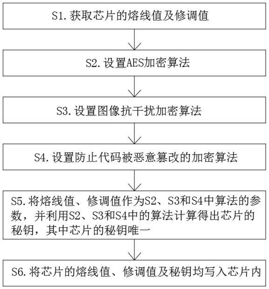
[0047] see figure 1 , the present invention provides a kind of technical scheme: a kind of application method on encryption chip based on AES encryption algorithm, comprises the following steps:

[0048] S1. Obtain the fuse value and trimming value of the chip;

[0049] S2. Setting the AES encryption algorithm;

[0050] S3. Setting the image anti-jamming encryption algorithm;

[0051] S4. Set an encryption algorithm to prevent the code from being maliciousl...


PUM


Abstract

The invention discloses a method for applying an AES-based encryption algorithm to an encryption chip. The method comprises the following steps: S1, acquiring a fuse value and a trimming value of thechip; S2, setting an AES encryption algorithm; S3, setting an image anti-interference encryption algorithm; S4, setting an encryption algorithm for preventing the code from being maliciously tampered;S5, taking the fuse value and the trimming value as parameters of the algorithms in S2, S3 and S4, and calculating the secret key of the chip by using the algorithms in S2, S3 and S4, the secret keyof the chip being unique; and S6, writing the fuse value, the trimming value and the secret key of the chip into the chip. Parameters of a chip algorithm are adjusted by writing trimming values and fuse values of chips into the chips, and the trimming values and the fuse values are written into the chips as parameters of a calculation secret key algorithm due to the fact that the trimming values and the fuse values of the chips are slightly different in the actual production process. Therefore, the uniqueness of the secret key of the chip is ensured, and the safety and reliability of chip encryption are improved.

Description

technical field [0001] The invention belongs to the technical field of encryption algorithms, and in particular relates to an application method based on an AES encryption algorithm on an encryption chip. Background technique [0002] The basic process of data encryption is to process the original plaintext file or data according to a certain algorithm, making it an unreadable piece of code called "ciphertext", so that the original text can only be displayed after entering the corresponding key. In this way, the purpose of protecting data from being stolen and read by illegal persons is achieved. The reverse process of this process is decryption, that is, the process of converting the coded information into its original data), however, there are still various problems in the various application methods based on the AES encryption algorithm on the encryption chip on the market. [0003] A kind of database encryption method based on AES algorithm is disclosed as authorized an...

Claims


Application Information

Patent Timeline
IPC IPC(8): H04L9/06H04L29/08
CPCH04L9/0631H04L67/34
Inventor 叶新忠
Owner 上海桂垚信息科技有限公司
Features
  • R&D
  • Intellectual Property
  • Life Sciences
  • Materials
  • Tech Scout
  • Unparalleled Data Quality
  • Higher Quality Content
  • 60% Fewer Hallucinations
Learn More