Display panel, binding method thereof and display device

A display panel and binding technology, applied in the direction of identification devices, instruments, electrical components, etc., can solve problems such as indentation, and achieve the effect of dispersing pressure, reducing pressure, and increasing contact area

Pending Publication Date: 2021-02-26
WUHAN CHINA STAR OPTOELECTRONICS SEMICON DISPLAY TECH CO LTD
View PDF13 Cites 1 Cited by
  • Summary
  • Abstract
  • Description
  • Claims
  • Application Information

AI Technical Summary

Problems solved by technology

[0005] The purpose of the present invention is to provide a display panel, its binding method, and a display device to solve the problem of indentation caused by the pressure of the indenter during the Bending process in the prior art

Method used


Image

  • Display panel, binding method thereof and display device
  • Display panel, binding method thereof and display device
  • Display panel, binding method thereof and display device

Examples


Embodiment 1

[0041] In an embodiment of the present invention, a binding method of the display panel 100 is provided, and the binding method includes the following steps:

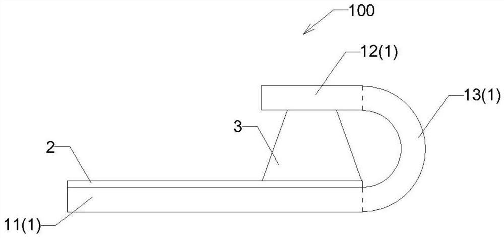
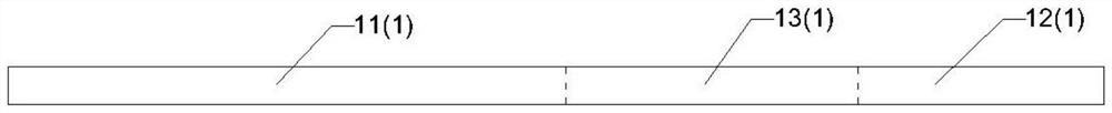
[0042] Step S10) provide a display layer 1: as figure 2 As shown, the display layer 1 has a display area 11 , a binding area 12 and a bending area 13 connecting the display area 11 and the binding area 12 .

[0043] Step S20) forming the heat dissipation layer 2: attaching a layer of metal material with excellent thermal conductivity on the back of the display layer 1, such as copper, silver, aluminum, etc., to form the heat dissipation layer 2, and the heat dissipation layer 2 corresponds to in the display area 11.

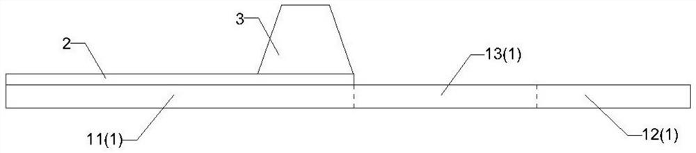
[0044] Step S30) form pasting layer 3: as image 3 As shown, an adhesive layer 3 is formed on a surface of the heat dissipation layer 2 away from the display area 11 of the display layer 1, and the adhesive layer 3 is a foam material, which is a table-shaped body. Specifically, the area of ​​the side o...

Embodiment 2

[0047] In an embodiment of the present invention, a binding method of the display panel 100 is provided, and the binding method includes the following steps:

[0048] Step S10) provide a display layer 1: as figure 2 As shown, the display layer 1 has a display area 11 , a binding area 12 and a bending area 13 connecting the display area 11 and the binding area 12 .

[0049] Step S20) forming the heat dissipation layer 2: attaching a layer of metal material with excellent thermal conductivity on the back of the display layer 1, such as copper, silver, aluminum, etc., to form the heat dissipation layer 2, and the heat dissipation layer 2 corresponds to in the display area 11.

[0050] Step S30) form pasting layer 3: as Figure 5 As shown, an adhesive layer 3 is formed in the adhesive layer formed on the back of the display layer 1 and corresponding to the binding area 12, and the adhesive layer 3 is a foam material, which is a table-shaped body. Specifically, the area of ​​the ...


PUM


Abstract

The invention provides a display panel, a binding method thereof and a display device. The display panel comprises a display layer, a heat dissipation layer and an adhesive layer. The display layer isprovided with a display area, a binding area and a bending area connected with the display area and the binding area. The heat dissipation layer is arranged on one surface of the display layer and corresponds to the display area. And the bonding layer is arranged between the heat dissipation layer and the binding area. The contact area between the bonding layer and the binding area is smaller than the contact area between the bonding layer and the heat dissipation layer.

Description

technical field [0001] The invention relates to the field of optical display devices, in particular to a display panel, a binding method thereof, and a display device. Background technique [0002] With the development and maturity of flexible organic light-emitting device (Organic Light-Emitting Diode, OLED) display technology, borderless OLED display has become one of the important development trends at present. In the manufacturing process of the borderless OLED display, pad bending (Pad Bending) technology becomes one of the keys to determine the yield. [0003] At present, the Pad Bending technology has gradually replaced the COF Bending technology and has become the mainstream Bending technology because it can significantly shorten the frame width of the display panel. The Pad Bending technology needs to cut the display substrate in a special shape, remove the test area of ​​the display substrate, and bend the Pad area to the back of the display substrate to reduce th...

Claims


Application Information

Patent Timeline
Patent Type & Authority Applications(China)
IPC IPC(8): H01L27/32H01L23/367H01L23/373G09F9/30
CPCH01L23/367H01L23/3736G09F9/301H10K59/10
Inventor 刘朗
Owner WUHAN CHINA STAR OPTOELECTRONICS SEMICON DISPLAY TECH CO LTD
Why Eureka
Try Eureka