A plasma etching method for large-diameter optical components

An optical element and plasma technology, applied in electrical elements, circuits, discharge tubes, etc., can solve the problems of inability to process medium and large-diameter optical elements, prolong the processing cycle, increase time and economic cost, and solve the surface residual stress and Subsurface damage, increased control dimension and control margin, and the effect of high-efficiency etch removal

Active Publication Date: 2022-08-02
XIAN TECH UNIV
View PDF6 Cites 0 Cited by
  • Summary
  • Abstract
  • Description
  • Claims
  • Application Information

AI Technical Summary

Problems solved by technology

However, it has been found in specific engineering practice that although PACE technology has extremely high work efficiency in eliminating defect layers on the surface and subsurface of components, due to the limitation of the size of the plasma generator electrode and the problem of plasma uniformity, this technology It is not yet possible to process medium and large aperture optical components
Atmospheric pressure plasma method can use computer control technology to process non-destructive processing of large-aperture optical components from point to point in the atmospheric environment. Unstable, unable to achieve deterministic removal of materials, and the secondary adsorption of products after chemical reactions on the surface of optical components will greatly affect the surface quality of components, reduce processing efficiency, and need to be assisted by other conformal processing methods for secondary adsorption Deposits are removed, thereby prolonging the processing cycle, resulting in an increase in time and economic costs

Method used


Image

  • A plasma etching method for large-diameter optical components
  • A plasma etching method for large-diameter optical components
  • A plasma etching method for large-diameter optical components

Examples


Embodiment 1

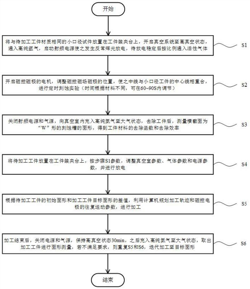
[0030] see figure 1 , a kind of plasma etching method provided by the invention comprises the following steps:

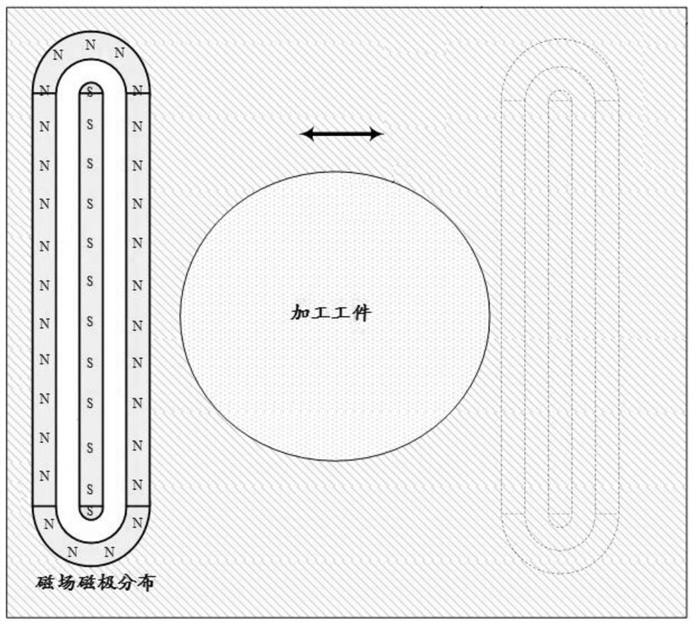
[0031] Step 1: Place the roughly ground fused silica optical specimen on the workpiece clamping table in the vacuum chamber, turn on the vacuum pump set connected to the vacuum chamber, and pump the vacuum chamber to 8.0×10 -4 Pa, introduce high-purity argon gas into the processing area of ​​the optical element of the vacuum chamber through the gas distributor (the gas distributor is located directly above the optical element, keep the centerlines of the two coincident), control the working vacuum of the vacuum chamber to 1Pa, and turn on the cooling water pair. The component clamping table is cooled, and the radio frequency power supply is turned on to discharge. After the discharge is stable, carbon tetrafluoride (CF 4 ) and oxygen (O 2 ), the working vacuum is 1Pa, the mass flow ratio of argon and carbon tetrafluoride is controlled at 1:1, and the oxygen ratio ...

Embodiment 2

[0046] The processing object is silicon carbide components, and the active gases introduced are sulfur hexafluoride and oxygen, and its mass flow ratio to argon can be formulated as Ar:SF 6 :O 2 It is 5:5:1, and other steps are the same as in Example 1.

Embodiment 3

[0048] The processing element is made of metal aluminum. In step 1, argon gas is introduced, and the working vacuum can be controlled at 0.6~1Pa, which is 1Pa in this embodiment. The etching time in step 2 is 60S, and other steps are the same as those in embodiment 1.


PUM

PropertyMeasurementUnit
diameteraaaaaaaaaa

Abstract

The invention discloses a plasma etching method for large-diameter optical components. The method draws on the radio frequency anomalous glow discharge method in the radio frequency magnetron sputtering coating technology, and can form high-density and large-area plasma. The directional movement of the orthogonal magnetic field can drive the plasma to produce directional movement, and realize the processing of the optical element surface by line and surface. The introduction of active gas is ionized and excited, and the flow conductance field generated by the inherent gas distributor of the vacuum system is used to guide the free radicals to act on the surface of the workpiece, which will also improve the etching efficiency of the material. And through the parameters of the radio frequency electric field (such as power, etc.), the parameters of the magnetic field (such as the small changes of each magnetic pole, including the equilibrium and non-equilibrium modes and the speed of the directional movement of the magnetic poles, etc.), and gas-related parameters (including the type of gas, flow rate and Pressure, etc.), the type, density and distribution of plasma can be precisely regulated, and high-efficiency large-area plasma polishing of the surface of optical components is realized.

Description

technical field [0001] The invention relates to the technical field of plasma etching processing of optical elements and semiconductor materials, in particular to a plasma etching method for large-diameter optical elements. Background technique [0002] With the expansion of the size and aperture of optical components and the expansion of materials, it also brings a series of new challenges and problems, mainly in the following aspects, one is that the processing aperture reaches the meter level, and the "inertial confinement nuclear fusion" optical engineering Nearly 1,000 pieces of aspherical optical elements with a side length of 430×430mm are required. The largest optical element diameter in the Shenguang III high-power laser device can reach 630mm. The objective lens of the tactical laser weapon needs a Φ460mm aspherical optical lens, and the space detection system needs 900mm. For the above aspherical optical lenses, in 2018, Chinese scientists successfully developed a...

Claims


Application Information

Patent Timeline
Patent Type & Authority Patents(China)
IPC IPC(8): H01J37/32
CPCH01J37/32082H01J37/3266H01J37/32669H01J2237/334
Inventor 惠迎雪刘卫国张进徐均琪边寒寒杨梦熊弥谦陈智利
Owner XIAN TECH UNIV
Why Eureka
Try Eureka