Check patentability & draft patents in minutes with Patsnap Eureka AI!

Non-volatile memory device

A non-volatile, memory technology that can be used in memory systems, static memory, read-only memory, etc. to solve problems such as increasing chip size

Pending Publication Date: 2021-03-05
SAMSUNG ELECTRONICS CO LTD
View PDF1 Cites 0 Cited by
  • Summary
  • Abstract
  • Description
  • Claims
  • Application Information

AI Technical Summary

Problems solved by technology

The number of pass transistors connected to the word line may increase, increasing the die size

Method used


Image

  • Non-volatile memory device
  • Non-volatile memory device
  • Non-volatile memory device

Examples


Embodiment Construction

[0025] Hereinafter, embodiments will be described in detail with reference to the accompanying drawings.

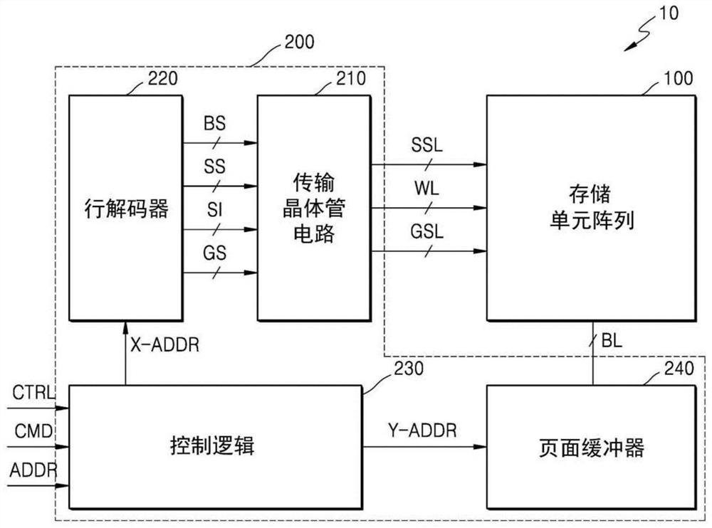
[0026] figure 1 is a block diagram of a memory device 10 according to some embodiments.

[0027] refer to figure 1 , the memory device 10 may include a memory cell array 100 and a peripheral circuit 200 . The peripheral circuit 200 may include a transfer transistor circuit 210 , a row decoder 220 , a control logic 230 and a page buffer 240 . Although not shown, peripheral circuit 200 may also include voltage generators, data input / output (I / O) circuits, I / O interfaces, column logic, pre-decoders, temperature sensors, command decoders, and / or address decoding device. In some embodiments, memory device 10 may be a non-volatile memory device. Hereinafter, the term "memory device" refers to a nonvolatile memory device.

[0028] In some example embodiments, at least a part of the pass transistor circuit 210 and the memory cell array 100 may be on the upper semiconductor ...


PUM


Abstract

A non-volatile memory device includes a memory cell region including a first metal pad and a memory cell array including a plurality of memory cells, and a peripheral circuit region including a secondmetal pad and vertically connected to the memory cell region. The memory cell region includes a plurality of word lines, a ground selection line in a layer on the word lines, a common source line ina layer on the ground selection line, a plurality of vertical pass transistors in the stair area, and a plurality of driving signal lines in the same layer as the common source line. The word lines form a stair shape in the stair area, and each of the vertical pass transistors is connected between a corresponding one of the word lines and a corresponding one of the driving signal lines.

Description

[0001] Cross References to Related Applications [0002] This application claims the benefit of Korean Patent Application No. 10-2019-0108469 filed with the Korean Intellectual Property Office on September 2, 2019, the entire disclosure of which is hereby incorporated by reference. technical field [0003] The inventive concept relates to a memory device, and more particularly, to a nonvolatile memory device having a cell on peripheral (COP) structure. Background technique [0004] With recent multifunctionalization of information and communication equipment, memory devices are expected to have high capacity and high integration density. As memory cell sizes are reduced to achieve high integration density, operating circuits and / or interconnect structures included in memory devices for operation and electrical connection of the memory devices become complex. Therefore, memory devices having high integration density and excellent electrical characteristics are desired. In p...

Claims


Application Information

Patent Timeline
IPC IPC(8): H01L27/11582G06F12/02G06F12/0882
CPCG06F12/0238G06F12/0882H10B43/27H01L27/0688H01L2224/08145G11C16/0483G11C16/08H01L25/0657H01L25/18H01L2225/06524H10B43/10H10B43/50H10B43/40H10B41/50H10B41/27H01L24/08H01L2924/1431H01L2924/14511
Inventor 金灿镐尹敬和边大锡
Owner SAMSUNG ELECTRONICS CO LTD
Features
  • R&D
  • Intellectual Property
  • Life Sciences
  • Materials
  • Tech Scout
  • Unparalleled Data Quality
  • Higher Quality Content
  • 60% Fewer Hallucinations
Learn More