A kind of cleaning method after gallium oxide wafer cmp
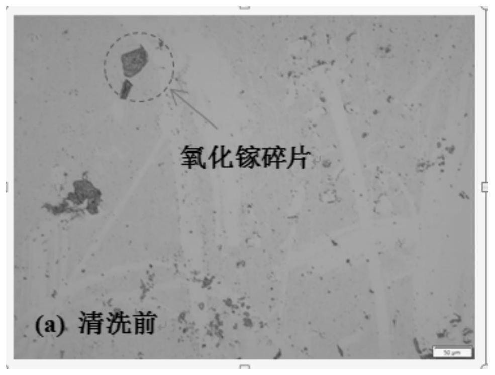
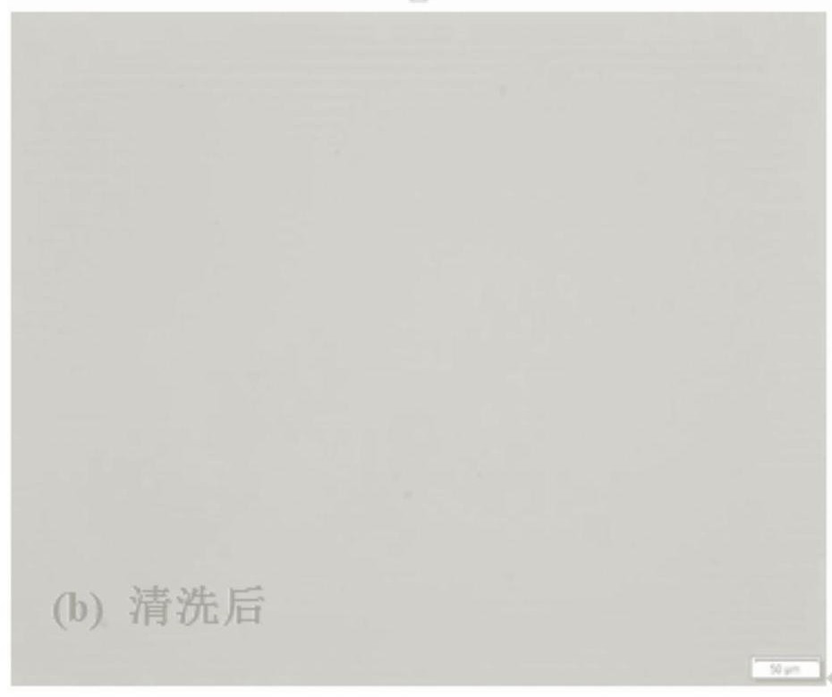
A gallium oxide and wafer technology, which is applied in the cleaning field of gallium oxide wafers after CMP, can solve problems such as bristle scratches and gallium oxide wafer damage, and achieve the effect of saving cleaning time and improving cleaning efficiency
- Summary
- Abstract
- Description
- Claims
- Application Information
AI Technical Summary
Problems solved by technology
Method used
Image
Examples
Embodiment 1
[0034] A cleaning method after gallium oxide wafer CMP comprises the steps:
[0035] S1. Clean the gallium oxide wafer after CMP with a cleaning solution I at a temperature of 80°C, and then wash it with deionized water; the cleaning solution I is composed of sulfuric acid, hydrogen peroxide and deionized water in a volume ratio of 2:1:8, Wherein, the concentration of sulfuric acid is 85%, and the concentration of hydrogen peroxide is 30%.
[0036] S2. Clean the gallium oxide wafer after cleaning in S1 with a cleaning solution II at a temperature of 50°C, and then clean it with deionized water; the cleaning solution II is composed of ammonia water, hydrogen peroxide and deionized water in a volume ratio of 2:1:10 , wherein the concentration of ammonia water is 20%, and the concentration of hydrogen peroxide is 30%.
[0037] S3. Clean the gallium oxide wafer after cleaning in S2 with a cleaning solution III at a temperature of 10°C, and then clean it with deionized water; the ...
Embodiment 2
[0041] A cleaning method after gallium oxide wafer CMP comprises the steps:
[0042] S1. Clean the gallium oxide wafer after CMP with a cleaning solution I at a temperature of 150°C, and then wash it with deionized water; the cleaning solution I is composed of sulfuric acid, hydrogen peroxide and deionized water in a volume ratio of 2:2:10, Wherein, the concentration of sulfuric acid is 85%, and the concentration of hydrogen peroxide is 30%.
[0043] S2. Clean the gallium oxide wafer after cleaning in S1 with cleaning solution II at a temperature of 100°C, and then clean it with deionized water; cleaning solution II is composed of ammonia water, hydrogen peroxide and deionized water in a volume ratio of 1:4:8 , wherein the concentration of ammonia water is 20%, and the concentration of hydrogen peroxide is 30%.
[0044] S3. Clean the gallium oxide wafer after cleaning in S2 with a cleaning solution III at a temperature of 37° C., and then clean it with deionized water; the cl...
Embodiment 3
[0048] A cleaning method after gallium oxide wafer CMP comprises the steps:
[0049] S1. Clean the gallium oxide wafer after CMP with cleaning solution I at a temperature of 100°C, and then clean it with deionized water; cleaning solution I is composed of sulfuric acid, hydrogen peroxide and deionized water in a volume ratio of 1:2:9, Wherein, the concentration of sulfuric acid is 85%, and the concentration of hydrogen peroxide is 30%.
[0050] S2. Clean the gallium oxide wafer after cleaning in S1 with a cleaning solution II at a temperature of 65°C, and then clean it with deionized water; the cleaning solution II is composed of ammonia water, hydrogen peroxide and deionized water in a volume ratio of 1:1:4 , wherein the concentration of ammonia water is 20%, and the concentration of hydrogen peroxide is 30%.
[0051] S3. Clean the gallium oxide wafer after cleaning in S2 with a cleaning solution III at a temperature of 20° C., and then clean it with deionized water; the cle...
PUM
 Abstract
Description
Claims
Application Information
 - R&D Engineer
- R&D Manager
- IP Professional
- Industry Leading Data Capabilities
- Powerful AI technology
- Patent DNA Extraction
Browse by: Latest US Patents, China's latest patents, Technical Efficacy Thesaurus, Application Domain, Technology Topic, Popular Technical Reports.
© 2024 PatSnap. All rights reserved.Legal|Privacy policy|Modern Slavery Act Transparency Statement|Sitemap|About US| Contact US: help@patsnap.com


