A photoelectric angle sensor based on a two-dimensional material light-absorbing structure array

An angle sensor and two-dimensional material technology, applied in the direction of instruments, optical devices, measuring devices, etc., can solve the problems of no public documents, etc., and achieve the effect of increasing quality factor, improving sensitivity and reducing leakage rate

Active Publication Date: 2021-11-26
NAT UNIV OF DEFENSE TECH
View PDF8 Cites 0 Cited by
  • Summary
  • Abstract
  • Description
  • Claims
  • Application Information

AI Technical Summary

Problems solved by technology

[0005] Although two-dimensional material light-absorbing structures can achieve light absorption enhancement, researchers are currently focusing on how to achieve absorption enhancement and control the absorption bandwidth. If the two-dimensional material light-absorbing structure can be applied to the field of angle sensors, it will be realized The miniaturization of the photoelectric angle sensor improves the sensitivity and precision of the sensor, but there is no published literature related to the realization of the photoelectric angle sensor by using two-dimensional material light absorption structure

Method used


Image

  • A photoelectric angle sensor based on a two-dimensional material light-absorbing structure array
  • A photoelectric angle sensor based on a two-dimensional material light-absorbing structure array
  • A photoelectric angle sensor based on a two-dimensional material light-absorbing structure array

Examples


Embodiment Construction

[0031] The content of the present invention will be further explained and illustrated in detail below in conjunction with the accompanying drawings. However, the following drawings are only schematic diagrams of idealized implementation cases of the present invention. In order to clearly show the physical structure of the device of the present invention, the schematic diagrams should not be regarded as strictly reflecting the proportional relationship of geometric dimensions. Of course, the illustrated embodiments of the present invention should not be considered limited to the specific shapes of the regions shown in the drawings. In short, the drawings are schematic and should not be considered as limiting the scope of the invention.

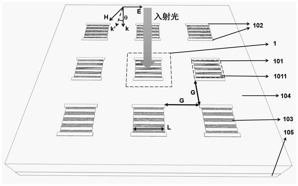
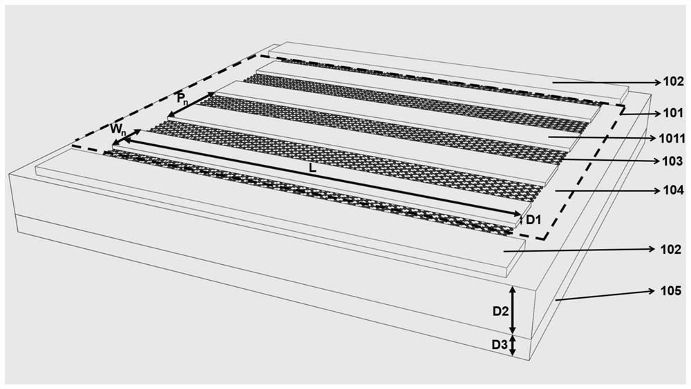
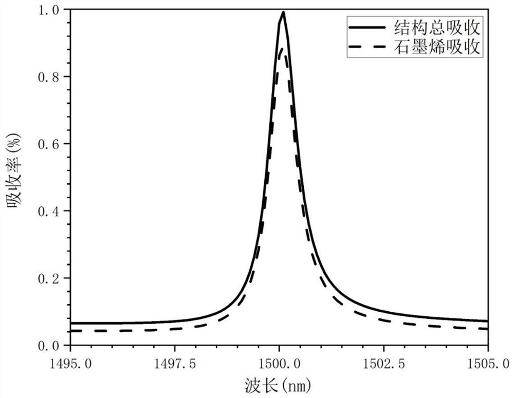
[0032] figure 1 It is a schematic diagram of the overall three-dimensional structure of Embodiment 1 of the present invention. The implementation of the present invention is based on a two-dimensional material light-absorbing structure array....


PUM

PropertyMeasurementUnit
thicknessaaaaaaaaaa
lengthaaaaaaaaaa
thicknessaaaaaaaaaa

Abstract

The invention discloses a photoelectric angle sensor based on a two-dimensional material light absorption structure array. The invention consists of a two-dimensional material light absorption structure array, and the array is composed of N two-dimensional material light absorption structure arrangements. The two-dimensional material light absorption structure is composed of an optically transparent dielectric grating, two metal electrodes, a two-dimensional material layer, an optical medium layer, and a metal film substrate. The period of the optically transparent dielectric grating of each two-dimensional material light absorption structure is different, so that each light absorption structure selectively absorbs light at different incident angles, and the electrical properties of the two-dimensional material change after absorbing light. The signal is converted into an electrical signal. The metal thin film substrate blocks the transmitted light to achieve zero leakage rate of the back mode, and the two-dimensional material is placed at a position with low field strength. The invention realizes the miniaturization of the photoelectric angle sensor and improves the sensitivity and precision of the sensor.

Description

technical field [0001] The invention relates to a photoelectric angle sensor, in particular to a photoelectric angle sensor based on a two-dimensional material light absorption structure array. Background technique [0002] Angle measurement is an important part of geometric metrology, and the measurement methods are mainly divided into mechanical angle measurement, electromagnetic angle measurement and optical angle measurement. Traditional angle sensors mainly include grating encoders, inductive synchronizers, resolvers and Hall elements. With the development of laser light sources, photoelectric materials and devices, the application of optical angle measurement technology is more and more extensive. It has the advantages of high measurement accuracy and non-contact measurement. Optical goniometric methods mainly include optical self-collimation method, optical internal reflection method, laser interferometry, ring laser method and so on. Although the angle sensors man...

Claims


Application Information

Patent Timeline
Patent Type & Authority Patents(China)
IPC IPC(8): G01B11/26
CPCG01B11/26
Inventor 郭楚才陈一鸣朱志宏袁晓东刘肯张检发
Owner NAT UNIV OF DEFENSE TECH
Why Eureka
Try Eureka