A kind of absorber of double split ring structure graphene
A technology of graphene and absorber, which is applied in the field of double-split ring structure graphene absorber, can solve the problems of limited bandwidth, insufficient absorption frequency band bandwidth, unfavorable application, etc., and achieve the effect of excellent robustness and superior absorption performance
- Summary
- Abstract
- Description
- Claims
- Application Information
AI Technical Summary
Problems solved by technology
Method used
Image
Examples
Embodiment 1
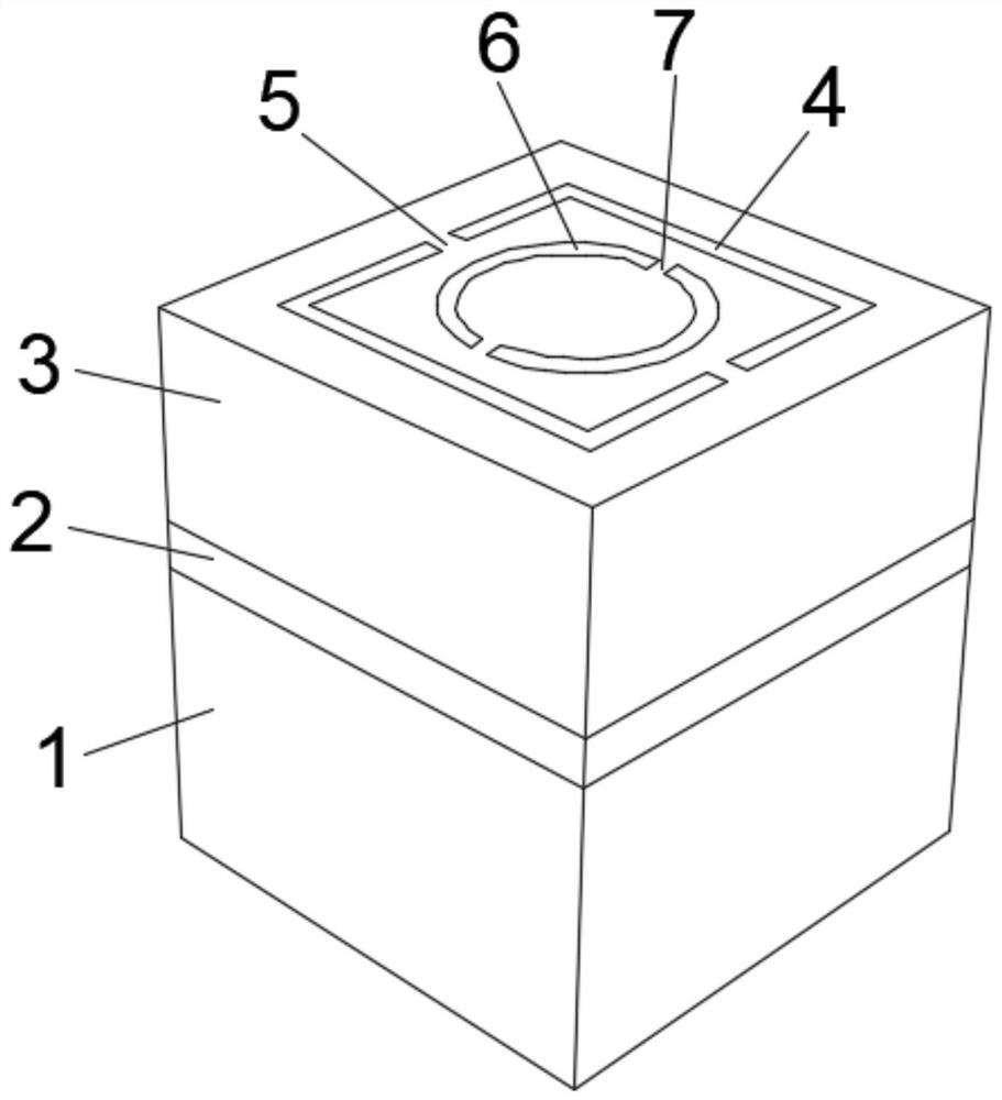
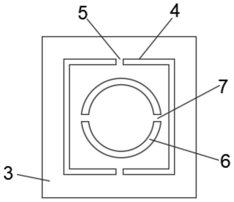
[0018] Example 1: A double crack ring structure graphene absorber, such as Figure 1-2 Shown, comprising a section of the square layer 1, a gold layer 2 and a silica layer 3 in descending cascading sequentially; the gold layer is an electroplated gold layer; the surface of the silica layer 3 is provided with a square crack ring of graphene 4, the middle of the square crack ring 4 is provided with two symmetrical first cracks 5; the surface of the silicon dioxide layer 3 is provided with a circular crack ring of material graphene 6, the circular crack ring 6 is provided with two symmetrical second cracks 7; the first crack 5 and the second crack 7 are perpendicular to each other. The thickness of the silica layer 3 is 4200nm, the length is 2450nm, the thickness of the gold layer 2 is 450nm, the length is 2450nm, the thickness of the silicon layer 3 is 2000nm, the length is 2450nm, the outer length of the square crack ring 4 is 1800nm, the inner length is 1600nm, the thickness is 1nm...
Embodiment 2
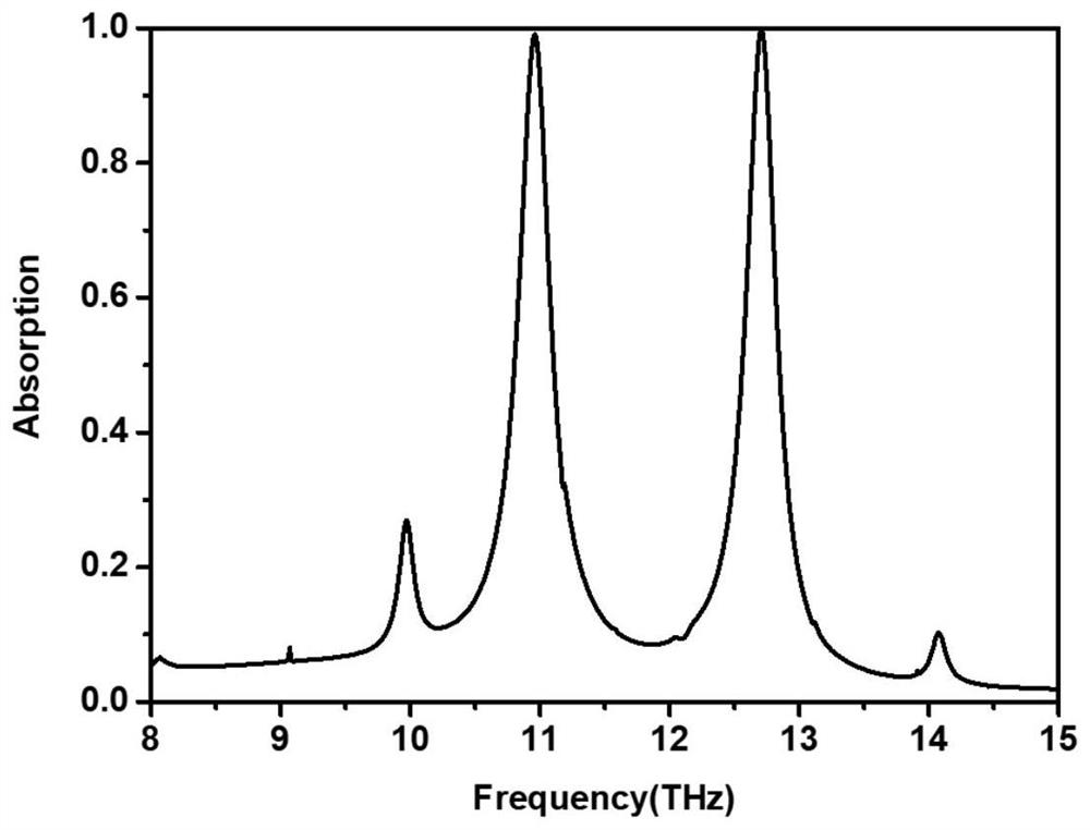
[0023] Example 2: On the basis of Example 1, the edges of the gold layer 2 are provided with a wavy topological boundary 8 in the middle; the four corners of the gold layer 2 are provided with a transmission hole lattice 9, and the transmission hole lattice at each corner 9 is a positive triangular matrix; the four transmissive hole lattices 9 constitute an array grid. By using the above knots, the spin state is obtained by superimposing the two polarization states based on the non-phase and inverted phase of terahertz waves. Topological phase transitions can be produced in the structure of the gold layer, resulting in better robustness. The applicant will be the absorber in Example 2 and the absorber in Example 1 into a comparison, for testing the absorption rate of terahertz, after testing, compared to the absorption effect in Example 1, the absorption rate in Example 2 may be further improved.
[0024] In summary, the absorber of the present invention comprises a square silicon...
PUM
| Property | Measurement | Unit |
|---|---|---|
| thickness | aaaaa | aaaaa |
| length | aaaaa | aaaaa |
| thickness | aaaaa | aaaaa |
Abstract
Description
Claims
Application Information


