External field guarantee and test platform for universal FC conversion interface module
A technology of converting interface and general interface, applied in the field of field support and test platform, can solve the problems of inability to meet product upgrade and test function requirements, single function of field support platform, no related test methods, etc., to achieve convenient operation and good scalability , the effect of simple structure
- Summary
- Abstract
- Description
- Claims
- Application Information
AI Technical Summary
Problems solved by technology
Method used
Image

Examples
Embodiment Construction
[0056] In order to make the purpose, technical solution and advantages of the present invention more clear, the embodiments of the present invention will be described in detail below in conjunction with the accompanying drawings. It should be noted that, in the case of no conflict, the embodiments in the present application and the features in the embodiments can be combined arbitrarily with each other.
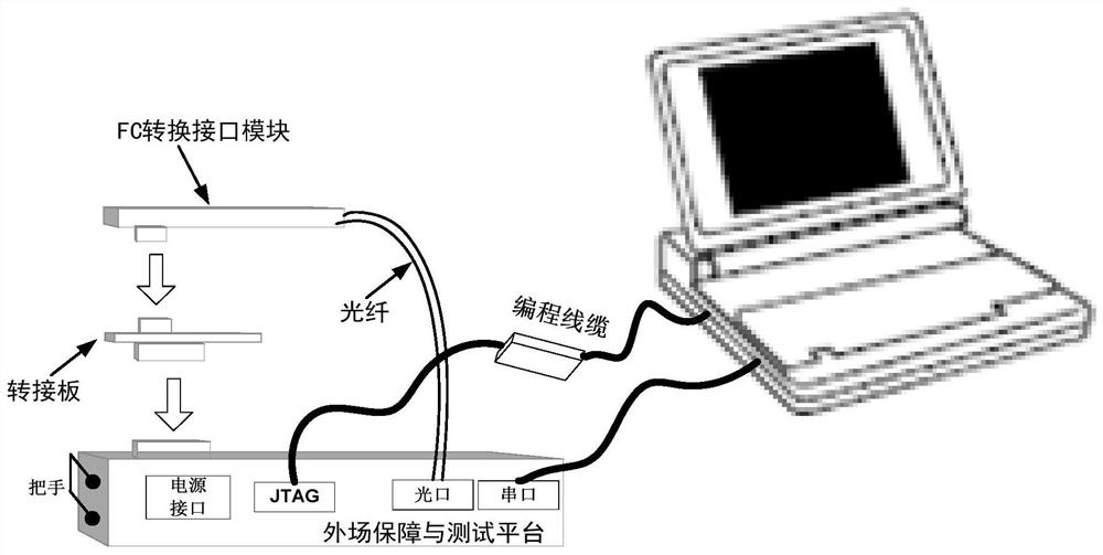
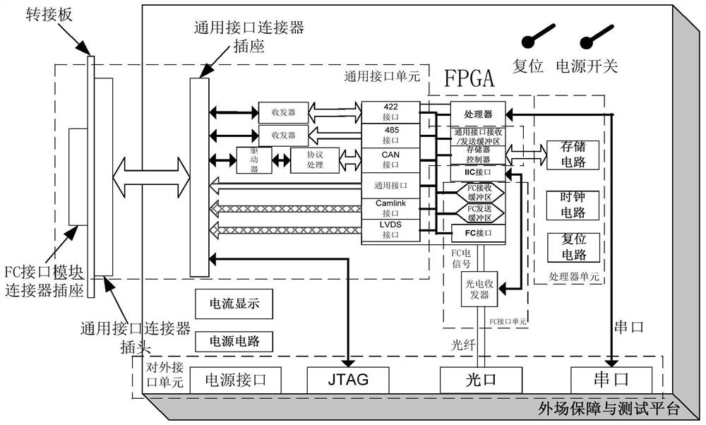
[0057] Aiming at the problems of the offline upgrade method of FC conversion interface module products in the background technology, that is, the field support platform has a single function, no relevant test means, and cannot meet the requirements of product upgrades and test functions in the field, a general-purpose method is innovatively proposed. The field support and test platform of the FC conversion interface module, the field support and test platform supports various types of FC conversion interface module products with common interfaces such as Camlink, LVDS, CAN, RS...
PUM
 Abstract
Description
Claims
Application Information