Burr positioning and burr detection model training method and device
A technology for detecting models and positioning methods, which is applied in the field of image recognition, and can solve problems such as glitch detection omissions, inability to cover, deformation of non-rigid O-shaped devices, etc.
- Summary
- Abstract
- Description
- Claims
- Application Information
AI Technical Summary
Problems solved by technology
Method used
Image
Examples
Embodiment 1
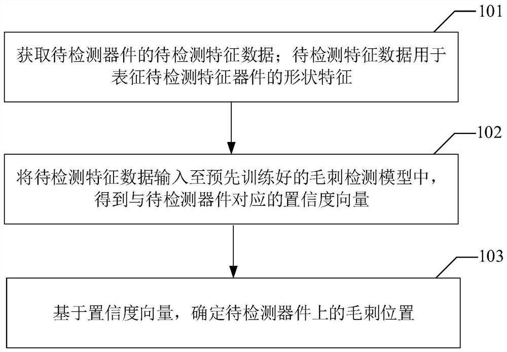
[0086] see figure 1 As shown, it is a schematic flow chart of a burr location method provided in the embodiment of the present application, which includes the following steps:
[0087] Step 101. Obtain the feature data to be inspected of the device to be inspected; the feature data to be inspected is used to characterize the shape characteristics of the feature device to be inspected.
[0088] Step 102: Input the feature data to be detected into a pre-trained glitch detection model to obtain a confidence vector corresponding to the device to be detected.
[0089] Step 103, based on the confidence vector, determine the position of the burr on the device to be tested.
[0090] The following is a detailed description of steps 101 to 103 .
[0091] For step 101:
[0092] When acquiring the feature data of the device to be detected, the image of the device to be detected can be obtained first, and the center point of the device to be detected and the edge of the device to be det...
Embodiment 2
[0129] The embodiment of the present application also provides a burr positioning device, see Figure 5 As shown, it is a schematic diagram of the structure of a burr location device provided by the embodiment of the present application, including a first acquisition module 501, a first detection module 502, and a first determination module 503, wherein the first detection module 502 includes a convolution unit 5021, feature fusion unit 5022, and upsampling unit 5023, specifically:
[0130] The first acquisition module 501 is configured to acquire the feature data to be detected of the device to be detected; the feature data to be detected is used to characterize the shape characteristics of the device to be detected;
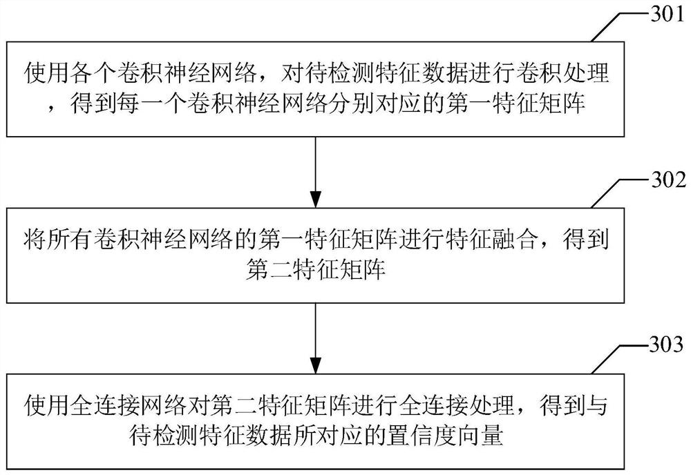
[0131] The first detection module 502 is configured to input the feature data to be detected into a pre-trained glitch detection model, the glitch detection model includes a plurality of convolutional neural networks and fully connected networks, different from...
Embodiment 3
[0163] Based on the same technical idea, an embodiment of the present application also provides an electronic device. refer to Figure 7 As shown, it is a schematic structural diagram of an electronic device 700 provided in the embodiment of the present application, including a processor 701 , a memory 702 , and a bus 703 . Among them, the memory 702 is used to store execution instructions, including a memory 7021 and an external memory 7022; the memory 7021 here is also called an internal memory, and is used to temporarily store calculation data in the processor 701 and exchange data with an external memory 7022 such as a hard disk. The processor 701 exchanges data with the external memory 7022 through the memory 7021. When the electronic device 700 is running, the processor 701 communicates with the memory 702 through the bus 703, so that the processor 701 executes the following instructions:
[0164] Obtaining the feature data to be detected of the device to be detected; t...
PUM
 Abstract
Description
Claims
Application Information


