Semiconductor substrate photoresist layer defect detection system based on AI and cloud computing technology

A photoresist layer and defect detection technology, which is applied in the direction of manufacturing computing systems, computing, computer components, etc., can solve the problems of poor real-time performance, poor detection effect, and low accuracy, so as to solve the problems of low manual detection efficiency and improve accuracy sex, efficiency-enhancing effect

Active Publication Date: 2022-03-01
重庆忽米网络科技有限公司
View PDF20 Cites 0 Cited by
  • Summary
  • Abstract
  • Description
  • Claims
  • Application Information

AI Technical Summary

Problems solved by technology

Existing substrate photoresist layer defect detection usually adopts manual detection method, which has low sampling rate, low accuracy, poor real-time performance, low efficiency, high labor intensity, and is greatly affected by manual experience and subjective factors problem, the detection effect is poor

Method used


Image

  • Semiconductor substrate photoresist layer defect detection system based on AI and cloud computing technology
  • Semiconductor substrate photoresist layer defect detection system based on AI and cloud computing technology
  • Semiconductor substrate photoresist layer defect detection system based on AI and cloud computing technology

Examples


Embodiment Construction

[0030] The present invention will be further described in detail below in conjunction with the accompanying drawings.

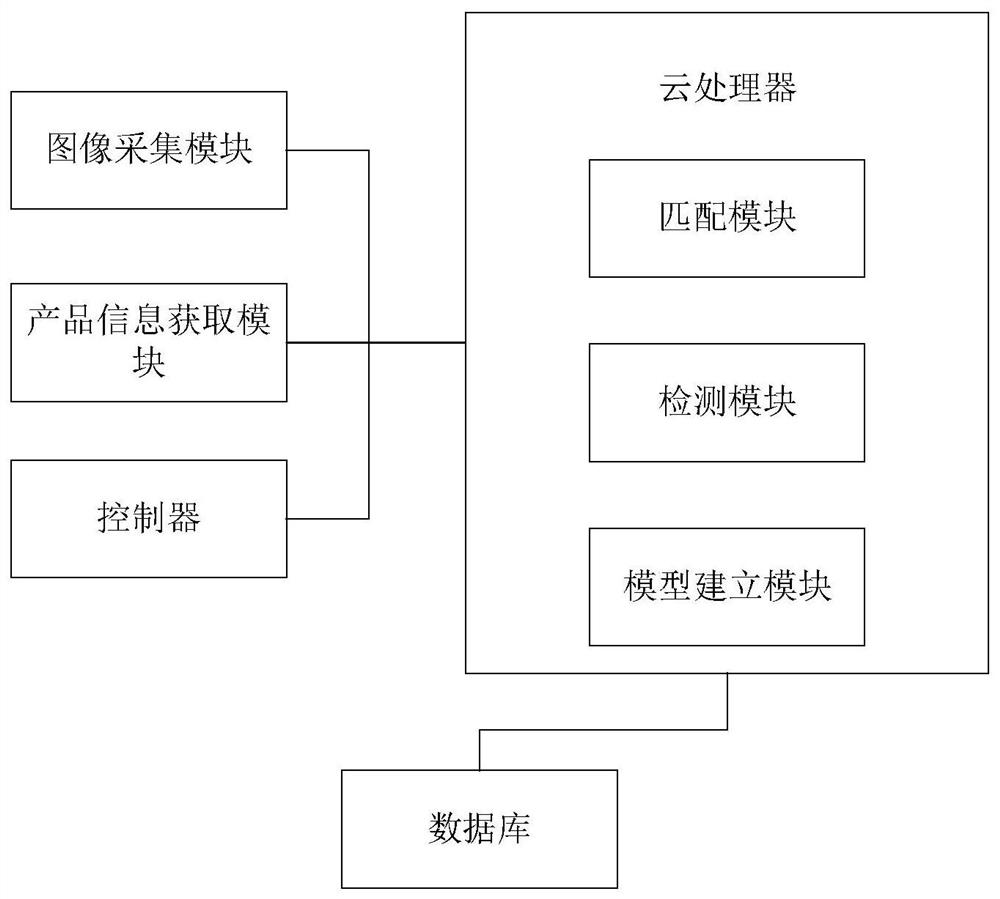
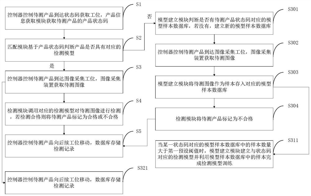
[0031] Such as figure 1 As shown, it is a schematic diagram of a semiconductor substrate photoresist layer defect detection system based on AI and cloud computing technology disclosed by the present invention, including a product information acquisition module, an image acquisition module, a cloud processor, a database, and a controller connected to each other through communication, The cloud processor includes a matching module and a detection module; such as figure 2 As shown, the AI ​​and cloud computing technology semiconductor substrate photoresist layer defect detection system includes the following steps when detecting:

[0032] S1. The controller controls the product to be tested to arrive at the status code acquisition station, and the product information acquisition module acquires the product status code of the product to be tested;

[0033] S2....


PUM


Abstract

The invention discloses a semiconductor substrate photoresist layer defect detection system based on AI and cloud computing technology, wherein the controller controls the product to be tested to arrive at the status code acquisition station, and the product information acquisition module acquires the product status code of the product to be tested; The module judges whether the product has a corresponding detection model based on the product status code. If so, the controller controls the product to be tested to arrive at the image acquisition station, and the image acquisition device acquires the image to be tested; the detection module calls the corresponding detection model to detect the image to be tested. If the test is qualified, the product to be tested is marked as qualified or unqualified; the controller controls the product to be tested to move to the subsequent station, and the database stores the test records. The invention adopts AI and cloud computing technology to realize automatic detection of photoresist layer defects, solve the problems of low efficiency, poor accuracy, and poor timeliness of manual detection of substrate photoresist layer surface defects, replace manual rapid inspection, and improve efficiency , reduce Chen cost, improve accuracy and other purposes.

Description

technical field [0001] The invention relates to the field of semiconductor technology, in particular to a semiconductor substrate photoresist layer defect detection system based on AI and cloud computing technology. Background technique [0002] Photoresists are organic compounds that change in solubility in developing solutions when exposed to ultraviolet light. The photoresist used in the manufacture of silicon wafers is applied to the surface of silicon wafers in liquid form and then dried to form a film. Photoresist is one of the key materials for micro-pattern processing in microelectronics technology, especially the development of large-scale and ultra-large-scale integrated circuits in recent years, which has greatly promoted the research, development and application of photoresist. [0003] In the pan-semiconductor field, the quality of the photoresist layer of the substrate directly affects the quality of the final product, so the defect detection of the photoresis...

Claims


Application Information

Patent Timeline
Patent Type & Authority Patents(China)
IPC IPC(8): G06T7/00G06K17/00G07C3/14G06Q10/06G06Q50/04
CPCG06T7/0004G06K17/00G07C3/143G06Q10/06395G06Q50/04G06T2207/20081G06T2207/20084G06T2207/30148Y02P90/30
Inventor 王成罗林郑静
Owner 重庆忽米网络科技有限公司
Why Eureka
Try Eureka