Chip packaging structure, chip packaging method and electronic equipment

A chip packaging structure and chip packaging technology, applied in circuits, electrical components, electrical solid devices, etc., can solve the problems of difficult to guarantee communication quality, long physical distance, large attenuation of intermediate frequency signals, etc., to shorten physical distance and reduce signal attenuation. , reduce the effect of attenuation

Inactive Publication Date: 2021-04-02
SHANGHAI WINGTECH INFORMATION TECH CO LTD
View PDF4 Cites 0 Cited by
  • Summary
  • Abstract
  • Description
  • Claims
  • Application Information

AI Technical Summary

Problems solved by technology

[0003] However, in related technologies, the millimeter-wave transceiver module and the millimeter-wave transceiver component communicate through a cable with a connector, and the physical distance between the two is relatively long, so the intermediate frequency signal transmitted between the two is greatly attenuated , making it difficult to guarantee the communication quality

Method used


Image

  • Chip packaging structure, chip packaging method and electronic equipment
  • Chip packaging structure, chip packaging method and electronic equipment
  • Chip packaging structure, chip packaging method and electronic equipment

Examples


no. 1 example

[0049] The chip packaging structure provided by the embodiments of the present invention can be used in various electronic devices involving millimeter wave transceivers, such as millimeter wave transceiver systems.

[0050] The specific structure of the chip packaging structure will be introduced below.

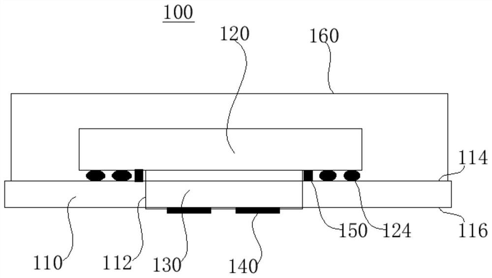
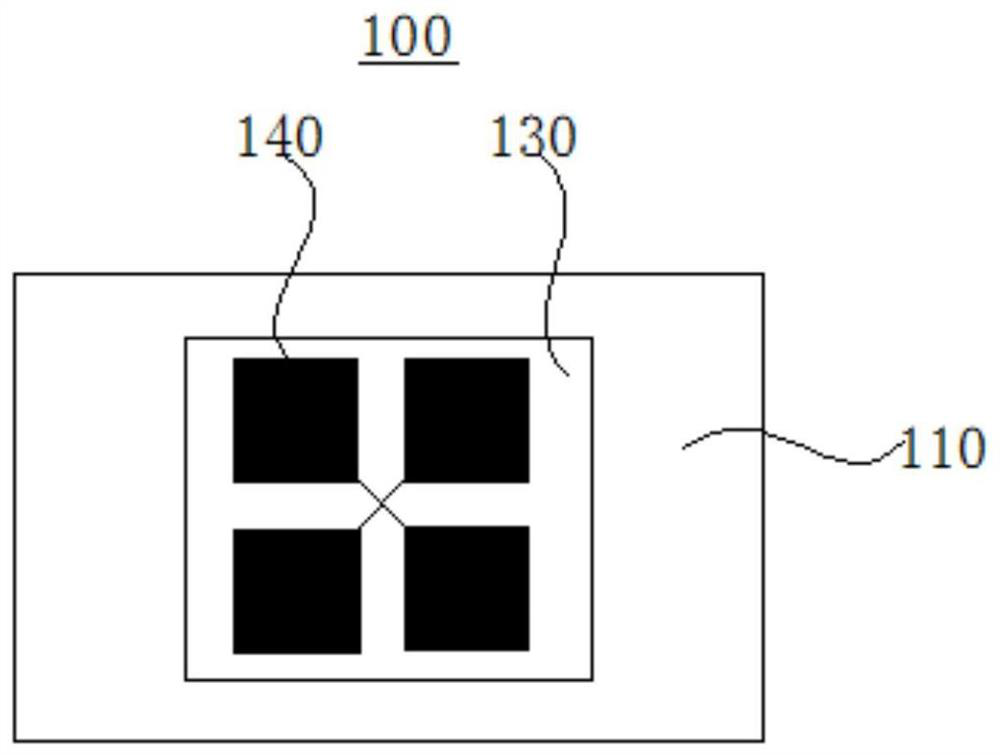
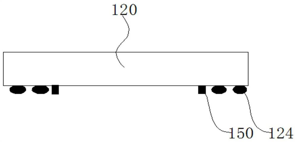
[0051] Please refer to figure 1 and figure 2 , the chip packaging structure 100 includes a substrate 110 , a first chip 120 , a second chip 130 and an antenna 140 . The first chip 120 is arranged on the substrate 110 and is electrically connected to the substrate 110, the second chip 130 is arranged on the first chip 120 and is electrically connected to the first chip 120, and the antenna 140 is arranged on the second chip 130 and is connected to the second chip. 130 electrical connection. The first chip 120 is used to output an intermediate frequency signal, the second chip 130 is used to process the intermediate frequency signal output by the first chip 120 to output a...

no. 2 example

[0076] Please refer to Figure 9 and Figure 10 , this embodiment also provides a chip packaging structure 100, its overall structure, working process and technical effects are basically the same as the chip packaging structure 100 provided in the first embodiment, the difference is that the substrate 110 and the second chip 130 relative positional relationship.

[0077] In this embodiment, the substrate 110 is no longer provided with the through hole 112, and the second chip 130 is arranged on the side of the first chip 120 away from the substrate 110. There is no need to set the shielding cover 160 on the top. Therefore, the chip packaging structure 100 provided by this embodiment has a simpler structure, and the corresponding manufacturing method is also simpler.


PUM


Abstract

The embodiment of the invention provides a chip packaging structure, a chip packaging method and electronic equipment, and relates to the technical field of chips; the chip packaging structure comprises a substrate, a first chip, a second chip and an antenna, the first chip is arranged on the substrate and electrically connected with the substrate, the second chip is arranged on the first chip andelectrically connected with the first chip, and the antenna is arranged on the second chip and is electrically connected with the second chip. The first chip is used for inputting or outputting intermediate-frequency signals, the second chip is used for converting the intermediate-frequency signals and millimeter-wave signals, and the antenna is used for transmitting or receiving the millimeter-wave signals. According to the chip packaging structure and the corresponding chip packaging method, the first chip and the second chip are integrated, so that the physical distance between the first chip and the second chip is shortened to a great extent, the attenuation of intermediate frequency signals propagated between the first chip and the second chip is effectively reduced, and the communication quality in the chip packaging structure is ensured. The electronic equipment comprises the chip packaging structure, and has the characteristics of small signal attenuation and high communication quality.

Description

technical field [0001] The present invention relates to the technical field of chips, in particular to a chip packaging structure, a chip packaging method and electronic equipment. Background technique [0002] Millimeter wave (millimeter wave) usually refers to electromagnetic waves with a wavelength of 1 to 10 mm. It is located in the wavelength range where microwaves and far-infrared waves overlap. Therefore, it has the characteristics of both spectrums and is widely used in 5G communications, radio astronomy and other fields. . The millimeter-wave transceiver system generally includes millimeter-wave transceiver modules, millimeter-wave transceiver components, and millimeter-wave antennas that are sequentially connected by communication. The conversion of the millimeter wave signal, the millimeter wave antenna is used to send and receive the millimeter wave signal. [0003] However, in related technologies, the millimeter-wave transceiver module and the millimeter-wave...

Claims


Application Information

Patent Timeline
Patent Type & Authority Applications(China)
IPC IPC(8): H01L23/31H01L23/66H01L23/58
CPCH01L23/3121H01L23/66H01L23/58H01L2223/6677
Inventor 何文卿
Owner SHANGHAI WINGTECH INFORMATION TECH CO LTD
Why Eureka
Try Eureka