Device for fixing seed crystal, growth device and method for rapid crystal growth
A crystal growth and rapid technology, applied in the direction of single crystal growth, single crystal growth, crystal growth, etc., can solve the problems of scrapped crystal frame, waste of materials, damaged crystal frame layer, etc., to achieve good universality without destroying stability. Effect
- Summary
- Abstract
- Description
- Claims
- Application Information
AI Technical Summary
Problems solved by technology
Method used
Image
Examples
Embodiment 1
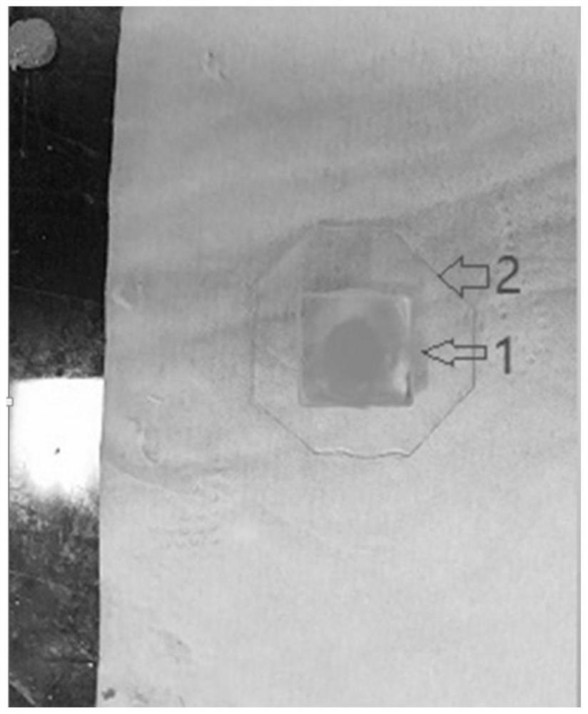
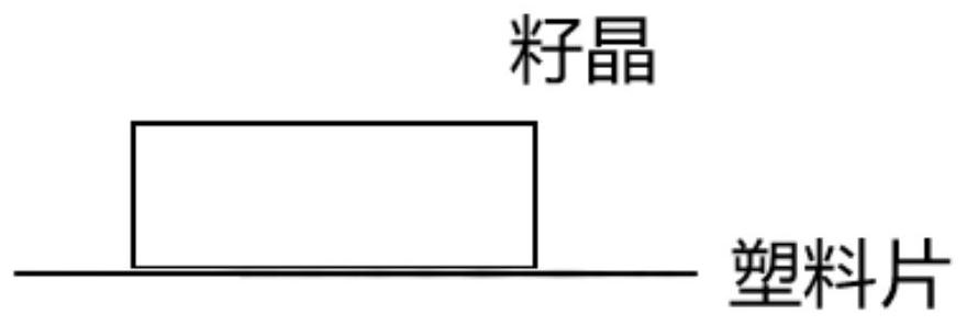
[0046] Such as image 3 Shown is a schematic diagram of the device for fixing the seed crystal, and the seed crystal is fixed on the upper surface of the plastic sheet. Such as Figure 4 As shown, it is a schematic diagram of a crystal growth device using a device for fixing the seed crystal. The seed crystal is fixed on the upper surface of the plastic sheet to form a device for fixing the seed crystal, which is placed in the middle of the crystal frame platform.
[0047] Such as figure 1 As shown, it is the physical picture of the device for fixing the seed crystal, in which 1 represents the seed crystal, which is a fast-growing seed crystal of 10×10×10 mm, and 2 represents a transparent plastic sheet, which is polygonal, with a friction coefficient of 0.45, a thickness of 1 mm, and a surface area of 9cm 2 , the fast-growing seed crystal 1 is glued on the plastic sheet 2 with AB glue.
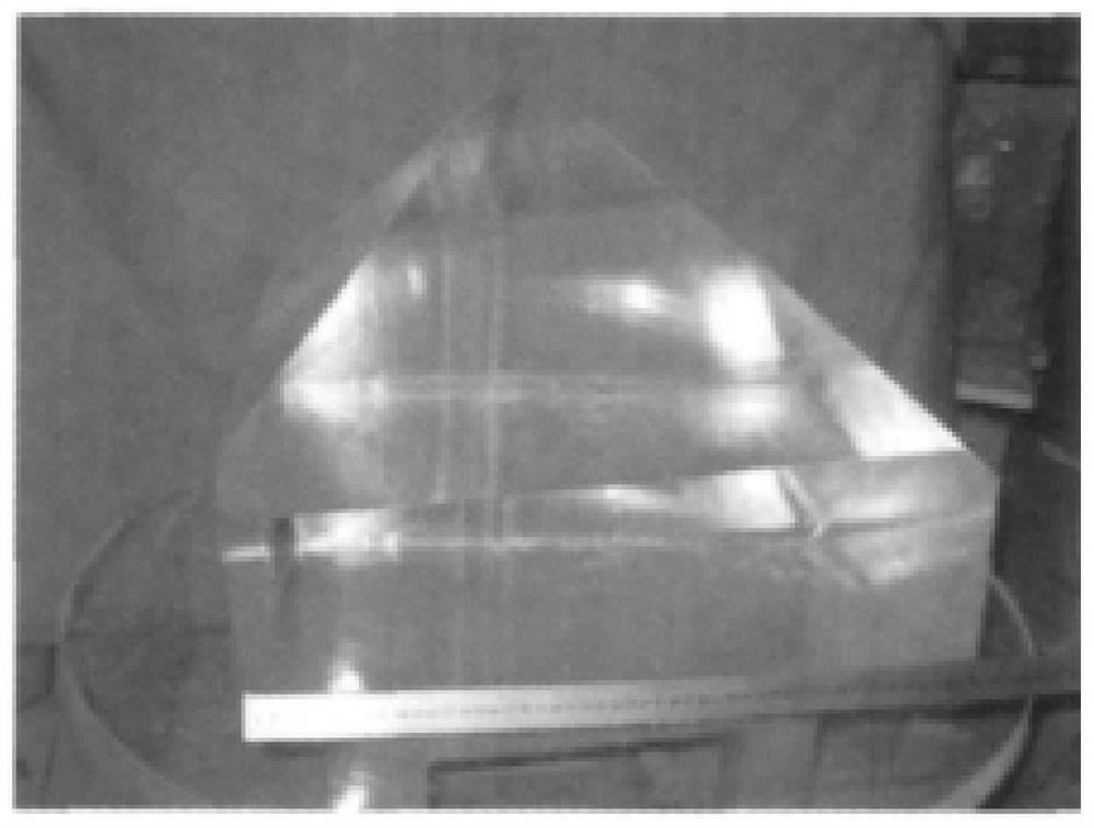
[0048] Such as figure 2 As shown, it is a KDP crystal rapidly grown by a crystal gr...
Embodiment 2
[0050] The device for fixing the seed crystal in Example 1 was used to grow KDP crystals. Inject seeds into the superheated growth saturated solution in the growth tank, and use a 1.5-meter stainless steel forceps to clamp the seed crystal and place it in the center of the crystal frame platform. After the seeding is completed, the KDP crystal grows stably and rapidly at a certain degree of supersaturation. Figure 5 It is the physical picture of KDP crystal obtained from the final growth, and the size is 100×100×60mm.
PUM
| Property | Measurement | Unit |
|---|---|---|
| thickness | aaaaa | aaaaa |
| surface area | aaaaa | aaaaa |
| thickness | aaaaa | aaaaa |
Abstract
Description
Claims
Application Information


