IGBT chip arrangement structure
A chip and heat sink technology, applied in the field of IGBT chip arrangement structure, can solve the problems of IGBT chip time difference, IGBT chip gate lead-out distance difference, IGBT chip current unbalance, etc., to achieve high reliability and current balance Good performance, good current flow
- Summary
- Abstract
- Description
- Claims
- Application Information
AI Technical Summary
Problems solved by technology
Method used
Image

Examples
Embodiment Construction
[0013] Specific embodiments of the present invention will be further described in detail below. It should be understood that the description of the embodiments of the present invention here is not intended to limit the protection scope of the present invention.
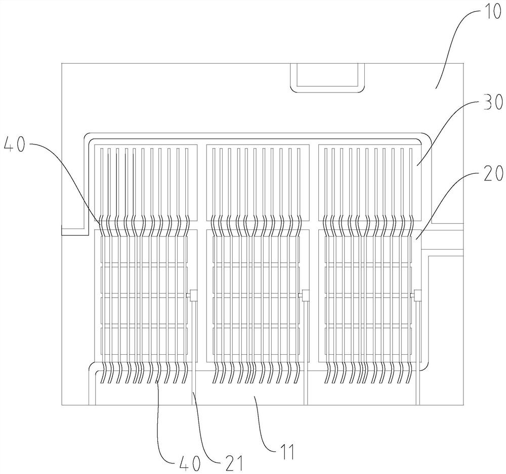
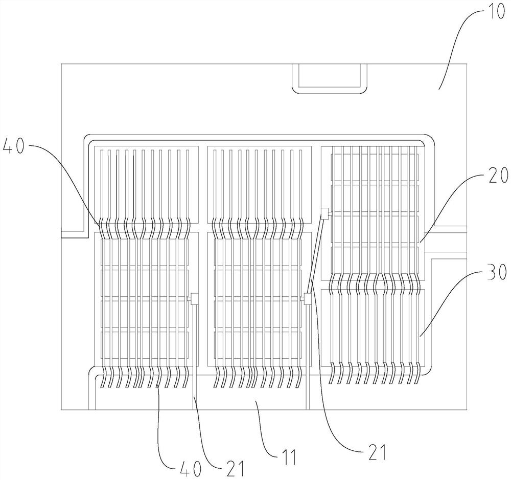
[0014] Such as figure 1 As shown, it is a structural schematic diagram of an IGBT chip arrangement structure provided by the present invention. An arrangement structure of IGBT chips 20, used to be arranged on a ceramic copper-clad substrate 10, the ceramic copper-clad substrate 10 includes a heat sink, including a plurality of IGBTs welded on the ceramic copper-clad substrate 10 and arranged in a straight line chip 20 and a plurality of diode chips 30, each of the diode chips 30 is bonded and connected to the corresponding IGBT chip 20 through a bonding aluminum wire 40 and is a group, and the gate of the IGBT chip 20 of each group is connected through a gate The electrode bonding aluminum wire 21 is bonded and con...
PUM
 Abstract
Description
Claims
Application Information
 - R&D
- Intellectual Property
- Life Sciences
- Materials
- Tech Scout
- Unparalleled Data Quality
- Higher Quality Content
- 60% Fewer Hallucinations
Browse by: Latest US Patents, China's latest patents, Technical Efficacy Thesaurus, Application Domain, Technology Topic, Popular Technical Reports.
© 2025 PatSnap. All rights reserved.Legal|Privacy policy|Modern Slavery Act Transparency Statement|Sitemap|About US| Contact US: help@patsnap.com