
Low-inductance crimping type semiconductor module
A crimping, semiconductor technology, applied in the direction of semiconductor devices, semiconductor/solid-state device components, electric solid-state devices, etc., can solve the problems of difficult to achieve, low thermal resistance, difficult to achieve circuit connection, etc., to reduce thermal resistance, improve the use of longevity, improving the effect of design redundancy
- Summary
- Abstract
- Description
- Claims
- Application Information
AI Technical Summary
Problems solved by technology
Method used
Image

Examples
Embodiment Construction
[0035] The present invention will be further described below in conjunction with the accompanying drawings. The following examples are only used to illustrate the technical solution of the present invention more clearly, but not to limit the protection scope of the present invention.
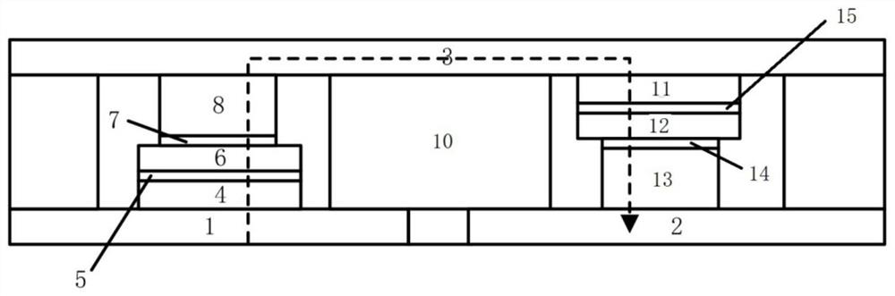
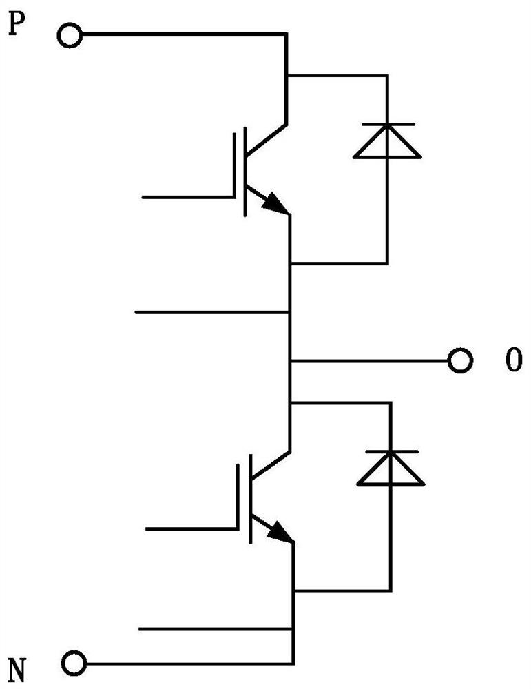
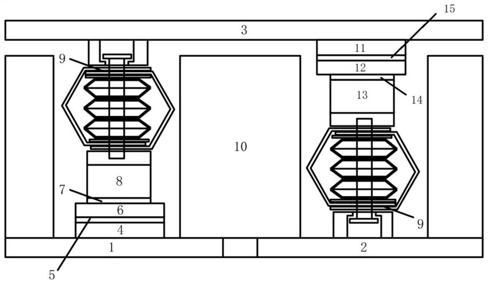
[0036] Specifically, as figure 1 with 2 As shown, a low-inductance crimping semiconductor module structure of the present invention includes: module upper bridge arm P pole 1, module lower bridge arm N pole 2, first chip drain conductor 4, second chip drain conductor 11 , the first chip and the drain conductor connection layer 5, the second chip and the drain conductor connection layer 15, the first power chip unit 6, the second power chip unit 12, the first chip and the source conductor connection layer 7, the second Chip and source conductor connection layer 14 , first chip source conductor 8 , second chip source conductor 13 , pressure-bearing limiting structure 10 , module output terminal ...
PUM
 Abstract
Description
Claims
Application Information