

Chip packaging structure and preparation method thereof
A packaging structure and chip technology, used in semiconductor/solid-state device manufacturing, electrical components, and electrical solid-state devices, etc., can solve problems such as deformation, short-circuit, and device performance failure of metal wires.
- Summary
- Abstract
- Description
- Claims
- Application Information
AI Technical Summary
Problems solved by technology
Method used
Image

Examples
preparation example Construction
[0037] In one aspect of the present invention, as figure 1 As shown, a method S100 for preparing a package structure of a chip is provided, and the method S100 includes:
[0038] S110, providing a carrier sheet.
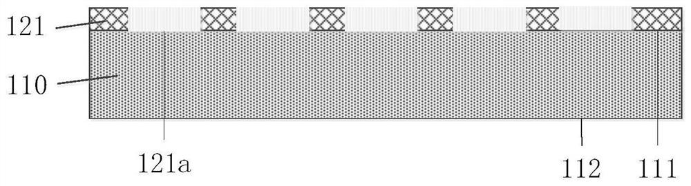
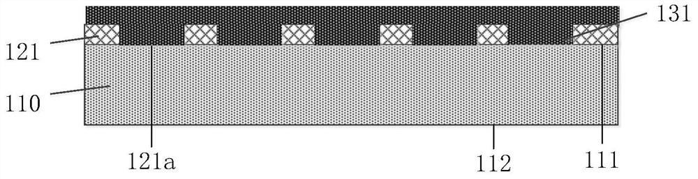
[0039] Exemplary, combined with figure 2 , providing a carrier sheet 110, the carrier sheet 110 includes a first surface 111 and a second surface 112 oppositely arranged along its thickness direction. In this step, the carrier sheet 110 can be a flat plate made of silicon, glass, metal, organic substrate, etc. Those skilled in the art can also choose carrier sheets of other materials according to actual needs, which is not limited in this embodiment.
[0040] S120, sequentially forming at least one first passivation layer and at least one second passivation layer on the first surface of the carrier sheet along its thickness direction, the second passivation layer and the first passivation layer Alternate interval settings.
[0041] Exemplarily, in this step, a l...
PUM
| Property | Measurement | Unit |
|---|---|---|
| thickness | aaaaa | aaaaa |
| thickness | aaaaa | aaaaa |
| width | aaaaa | aaaaa |
Abstract
Description
Claims
Application Information