Vertical gate structure and layout in CMOS image sensor

A gate and transfer gate technology, applied in the field of image sensors

Active Publication Date: 2021-04-16
OMNIVISION TECH INC
View PDF6 Cites 2 Cited by
  • Summary
  • Abstract
  • Description
  • Claims
  • Application Information

AI Technical Summary

Problems solved by technology

As the demand on image sensors continues to rise, the isolation of pixel cells in image sensors with high packing density and noise performance has become more and more challenging

Method used


Image

  • Vertical gate structure and layout in CMOS image sensor
  • Vertical gate structure and layout in CMOS image sensor
  • Vertical gate structure and layout in CMOS image sensor

Examples


Embodiment Construction

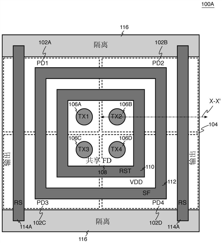
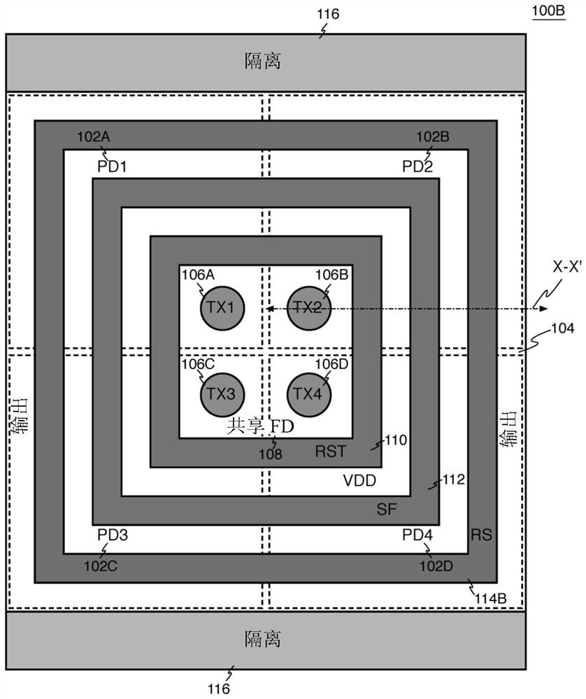
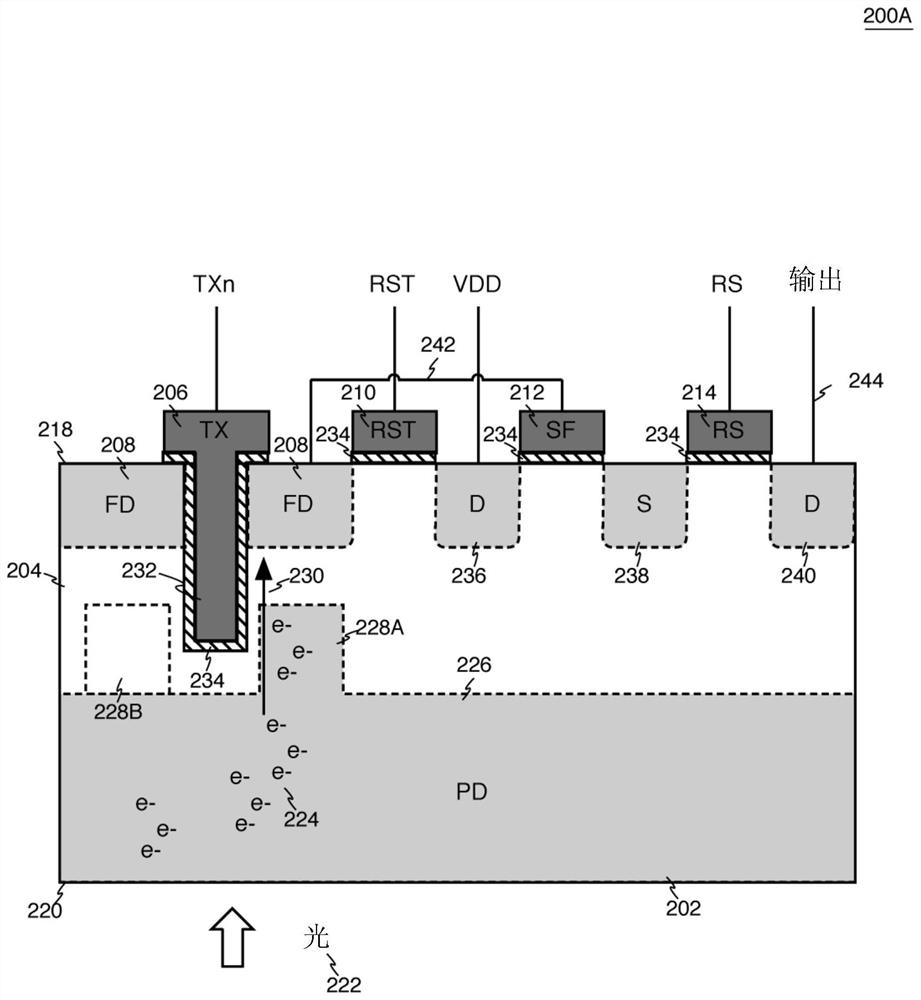
[0014] Devices directed to pixel cells with vertical gate structures are disclosed. In the following description, numerous specific details are set forth in order to provide a thorough understanding of the embodiments. One skilled in the relevant art will recognize, however, that the techniques described herein may be practiced without one or more of these specific details or may be practiced with other methods, components, materials, etc. In other instances, well-known structures, materials, or operations are not shown or described in detail to avoid obscuring certain aspects.

[0015] Reference throughout this specification to "one example" or "an embodiment" means that a particular feature, structure, or characteristic described in connection with the example is included in at least one example of the present invention. Thus, appearances of the phrase "in one instance" or "in one embodiment" in various places throughout this specification are not necessarily all referring ...


PUM


Abstract

The invention relates to a vertical gate structure and layout in a CMOS image sensor. A pixel cell includes a photodiode buried beneath a first side of semiconductor material and coupled to photogenerate image charge in response to incident light. A transfer gate is disposed over the photodiode and includes a vertical transfer gate portion extending a first distance from the first side into the semiconductor material. A floating diffusion region is disposed in the semiconductor material proximate to the transfer gate and is coupled to transfer the image charge from the photodiode toward the first side of the semiconductor material and into the floating diffusion region in response to a transfer control signal. A first pixel transistor having a first gate is disposed over the photodiode proximate to the first side of the semiconductor material. The first gate has a ring structure laterally surrounding the floating diffusion region and the transfer gate at the first side of the semiconductor material.

Description

technical field [0001] The present invention relates generally to image sensors, and more particularly to image sensor pixel cells having vertical gate structures. Background technique [0002] CMOS image sensors (CIS) have become ubiquitous. It is widely used in digital still cameras, cellular phones, security cameras, as well as in medical, automotive and other applications. Technology for manufacturing image sensors continues to advance rapidly. The need for higher resolution and lower power consumption has driven further miniaturization and integration of these devices. As the demands on image sensors continue to rise, the isolation of pixel cells in image sensors with high packing density and noise performance has become more and more challenging. Contents of the invention [0003] One aspect of the invention relates to a pixel cell comprising: a photodiode buried in a semiconductor material beneath a first side of the semiconductor material, wherein the photodiode...

Claims


Application Information

Patent Timeline
IPC IPC(8): H01L27/146
CPCH01L27/14605H01L27/14645H01L27/14607H01L27/1463H01L27/14614H01L27/1464H01L27/14641H01L27/14612
Inventor 臧辉陈刚
Owner OMNIVISION TECH INC
Why Eureka
Try Eureka