Eureka AIR delivers breakthrough ideas for toughest innovation challenges, trusted by R&D personnel around the world.

Wafer expanding device, wafer expanding apparatus and wafer processing method

A device and wafer technology, applied in the manufacturing of electrical components, electrical solid-state devices, semiconductor/solid-state devices, etc., can solve the problems of film peeling, uneven chip spacing, unfavorable chip operation, etc., to increase stability and simplify extension control. Steps, the effect of increasing the flexibility of operation

Pending Publication Date: 2021-04-30
东莞市瑞勤电子有限公司
View PDF0 Cites 0 Cited by
  • Summary
  • Abstract
  • Description
  • Claims
  • Application Information

AI Technical Summary

Problems solved by technology

[0003] However, in the case of using two inner and outer crystal expansion rings to clamp and fix the film, once the crystal expansion ring deforms, it is very easy to cause the film to fall off partially or completely from between the two crystal expansion rings, so that each film will shrink due to film shrinkage. The problem of uneven spacing between chips is not conducive to the subsequent operation of chips

Method used


Image

  • Wafer expanding device, wafer expanding apparatus and wafer processing method
  • Wafer expanding device, wafer expanding apparatus and wafer processing method
  • Wafer expanding device, wafer expanding apparatus and wafer processing method

Examples


Embodiment Construction

[0029] Hereinafter, the present invention will be described in more detail with reference to the accompanying drawings. In the various drawings, the same elements are denoted by the same or similar reference numerals. For the sake of clarity, various parts in the drawings have not been drawn to scale. Also, some well-known parts may not be shown. For the sake of simplicity, the semiconductor structure obtained after several steps can be described in one figure.

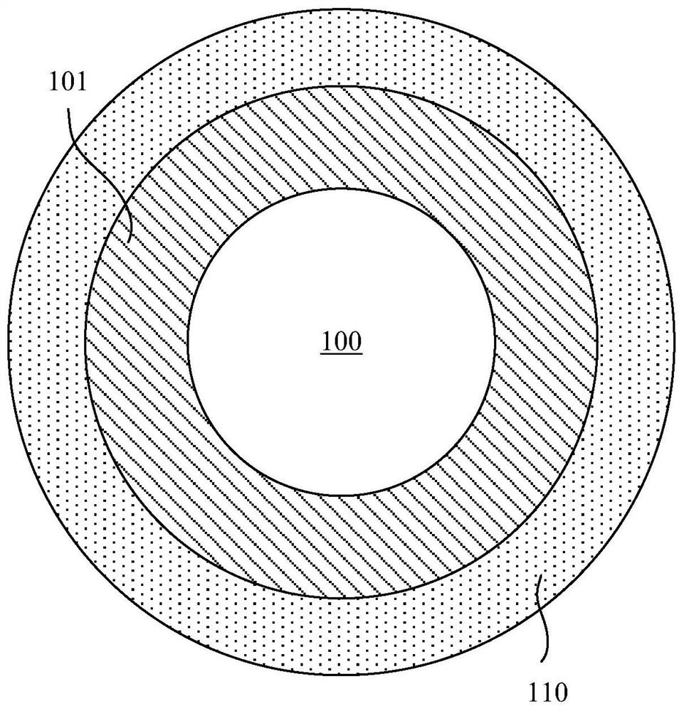
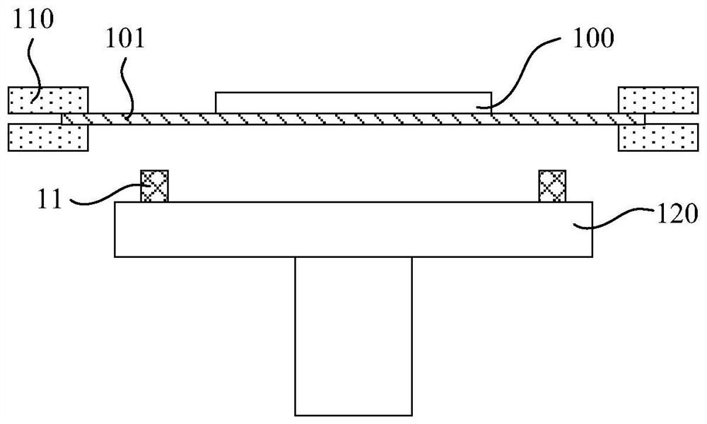
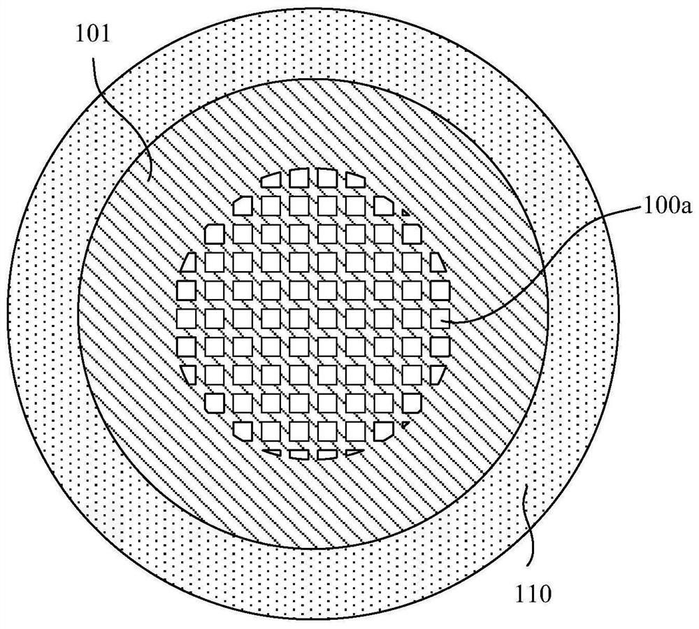
[0030] Figure 1a to Figure 4b is a schematic diagram of some stages of the wafer processing method in the related process, wherein, Figure 1a for Figure 1b top view of the Figure 2a for Figure 2b top view of the Figure 3a for Figure 3b top view of the Figure 4a for Figure 4b bottom view.

[0031] In the related process, the edge of the thin film 101 carrying the diced wafer 100 needs to be clamped and fixed by the clamping structure 110 first, and then the inner expansion ring 11 is placed on the to...


PUM


Abstract

The invention discloses a wafer expanding device, a wafer expanding apparatus and a wafer processing method, and the wafer expanding device comprises a first fixed ring which is fixedly connected with a first thin film, wherein the first thin film at least covers an area surrounded by an inner ring of the first fixed ring, and a bearing area of the first thin film is used for bearing a wafer; and a second fixed ring which is located on the first fixed ring and is fixedly connected with a second thin film, wherein the second thin film is provided with a hollowed-out area and an extending part, and the hollowed-out area is opposite to the bearing area of the first thin film, and the first thin film is extended, so that the bearing area moves along the direction from the first fixed ring to the second fixed ring, and the extending parts of the first film and the second film are contacted and fixed. According to the wafer expanding device, the extended first thin film is fixed by the second thin film, and a mode of fixing the thin film by using a wafer expanding ring is replaced, so that the stability of fixing the first thin film is improved.

Description

technical field [0001] The invention relates to the field of semiconductor device manufacturing, and more specifically, to a crystal expansion device, crystal expansion equipment and a wafer processing method. Background technique [0002] In the manufacturing process of semiconductor devices, operations such as detection and sorting are performed on the separated chips on the wafer after the wafer dicing step. In order to facilitate the detection and sorting operations, it is necessary to perform wafer expansion operations on the wafer. Specifically, the distance between each chip is enlarged by extending the film used to carry the wafer. After the film is stretched, two inner and outer plastic expansion rings are used to clamp and fix the stretched film, and the excess film is cut. [0003] However, in the case of using two inner and outer crystal expansion rings to clamp and fix the film, once the crystal expansion ring deforms, it is very easy to cause the film to fall o...

Claims


Application Information

Patent Timeline
IPC IPC(8): H01L21/683H01L21/67H01L21/78
CPCH01L21/67092H01L21/6836H01L21/78H01L2221/68336
Inventor 罗小虎陈为波张继栋曹诚
Owner 东莞市瑞勤电子有限公司
Why Eureka
Eureka Blog
Learn More