

Printed circuit board production and processing method
A technology of printed circuit boards and processing methods, which is applied in the directions of printed circuits, printed circuit manufacturing, and assembly of printed circuits with electrical components, and can solve problems such as easy movement, device wear, printed circuit board fixation, and difficult operation
- Summary
- Abstract
- Description
- Claims
- Application Information
AI Technical Summary
Problems solved by technology
Method used
Image

Examples
Embodiment Construction
[0044] The technical solutions in the embodiments of the present invention will be clearly and completely described below in conjunction with the accompanying drawings in the embodiments of the present invention. Obviously, the described embodiments are only some of the embodiments of the present invention, not all of them. Based on the embodiments of the present invention, all other embodiments obtained by persons of ordinary skill in the art without making creative efforts all belong to the protection scope of the present invention.
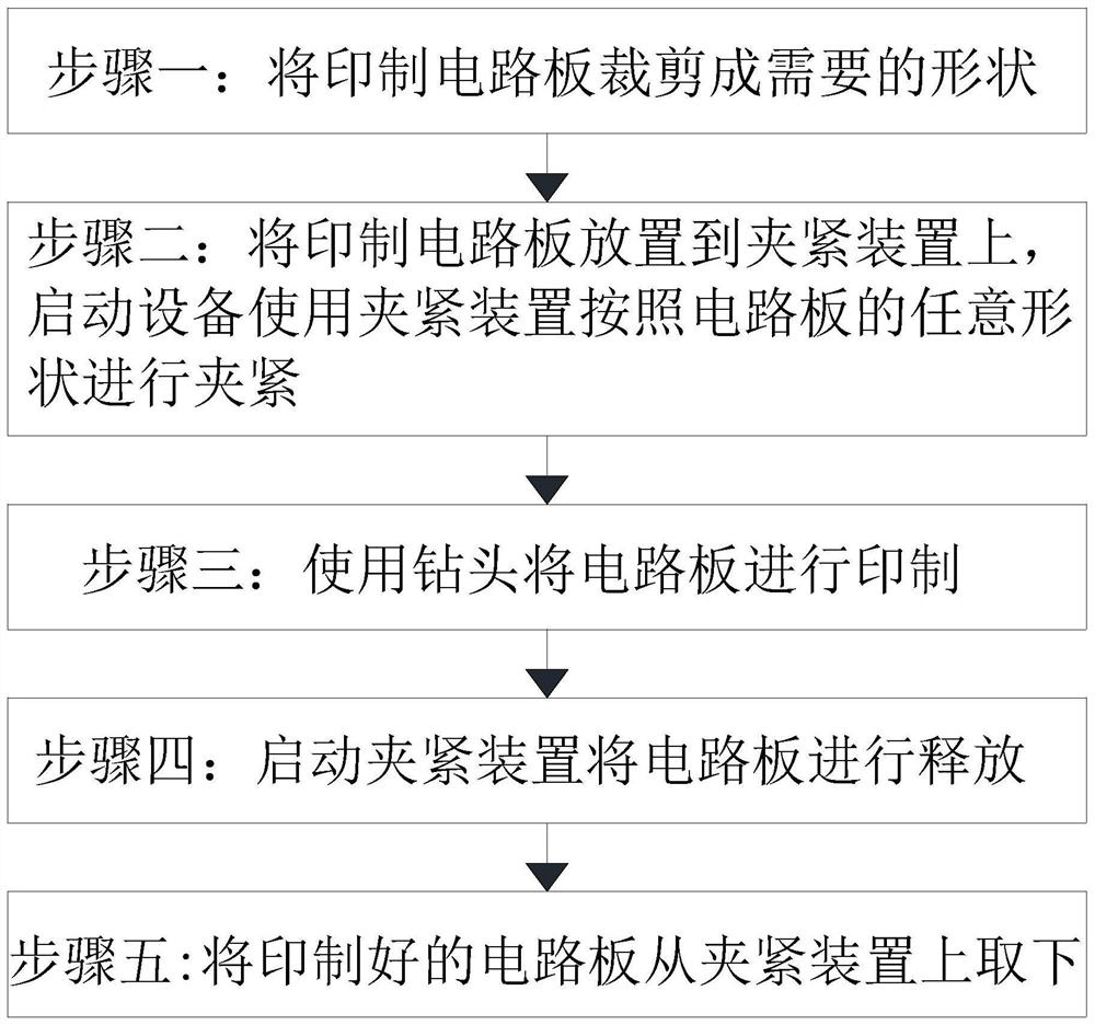
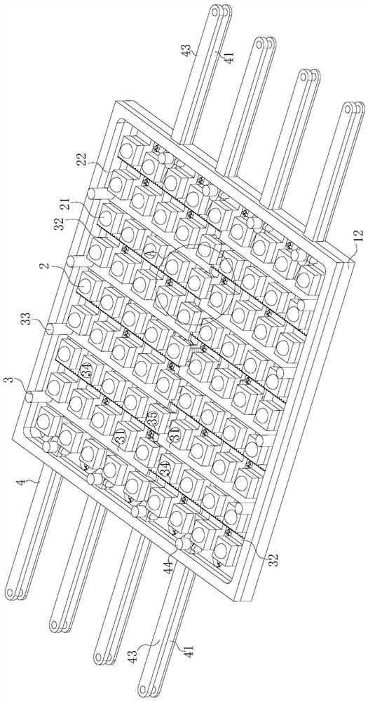
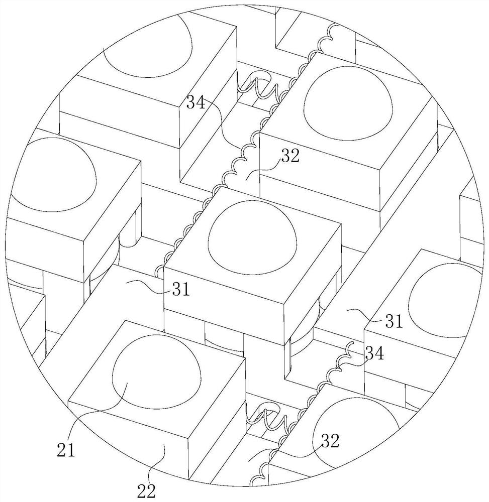
[0045] see Figure 1-14 , the present invention provides a kind of technical scheme: a kind of printed circuit board production and processing method, the concrete steps of this method are as follows:
[0046] Step 1: Cut the printed circuit board into the required shape;
[0047]Step 2: Place the printed circuit board on the clamping device, start the equipment and use the clamping device to clamp according to any shape of the circuit board; ...
PUM
 Abstract
Description
Claims
Application Information