Data transmission interface circuit and data transmission method thereof
A technology of data transmission interface and data transmission method, which is applied in the direction of electrical digital data processing, instruments, etc., can solve the problems of too many bus transceivers, waste of channel resources, and increased circuit complexity.
- Summary
- Abstract
- Description
- Claims
- Application Information
AI Technical Summary
Problems solved by technology
Method used
Image

Examples
Embodiment 1
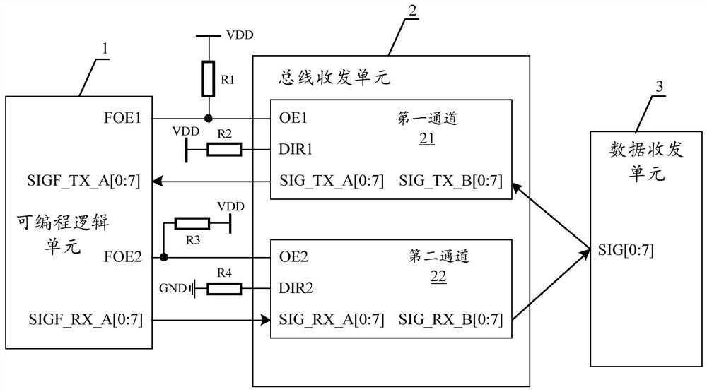
[0038] see figure 1, is a schematic diagram of the data transmission interface circuit provided by Embodiment 1 of the present invention. In this implementation, the data transmission interface circuit includes: a programmable logic unit 1, a first resistor R1, a second resistor R2, a third resistor R3, a fourth resistor R4, a bus transceiver unit 2, and a data transceiver unit 3, so The bus transceiver unit 2 includes a first channel 21 and a second channel 22 . In some of these embodiments, the programmable logic unit 1 is a Field Programmable Gate Array (Field Programmable Gate Array, FPGA), the bus transceiver unit is an in-phase bus transceiver (such as SN74ALVC164245 chip), and the data transceiver unit is Analog-to-digital converter (such as AD7712 chip).
[0039] In some of these embodiments, through an FPGA-based programmable gate array, the hardware VHDL language can be used to program and complete asynchronous bidirectional signal transmission (the program inside ...
Embodiment 2
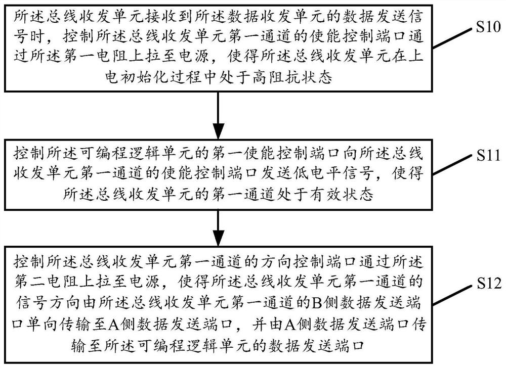
[0051] see figure 2 , is a data transmission flowchart of the data transmission method provided in Embodiment 2 of the present invention. In this embodiment, according to different requirements, figure 2 The order of execution of the steps in the flowcharts shown may be changed, and certain steps may be omitted. in, figure 2 The data transfer method shown applies to the figure 1 The data transmission interface circuit.
[0052] Step S10: When the bus transceiver unit 2 receives the data transmission signal of the data transceiver unit 3, control the enable control port (OE1) of the first channel 21 of the bus transceiver unit 2 to pass through the first resistor R1 Pull it to the power supply VDD, so that the bus transceiver unit 2 is in a high impedance state during the power-on initialization process, thereby reducing the power-on current of the bus transceiver unit 2 .
[0053] Step S11: Control the first enable control port (FOE1) of the programmable logic unit 1 t...
Embodiment 3
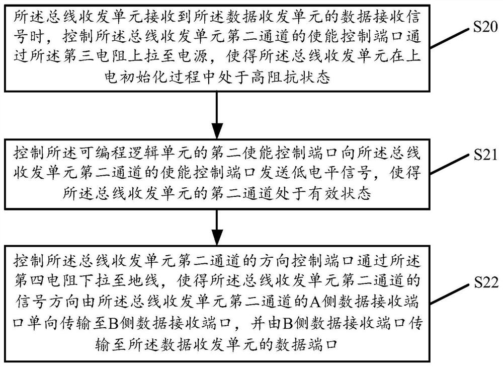
[0059] see image 3 , is a data receiving flowchart of the data transmission method provided in Embodiment 3 of the present invention. In this embodiment, according to different requirements, image 3 The order of execution of the steps in the flowcharts shown may be changed, and certain steps may be omitted. in, image 3 The data transfer method shown applies to the figure 1 The data transmission interface circuit.
[0060] Step S20: When the bus transceiver unit 2 receives the data transmission signal of the data transceiver unit 3, control the enable control port (OE2) of the second channel 22 of the bus transceiver unit 2 to pass through the third resistor R3 Pull it to the power supply VDD, so that the bus transceiver unit 2 is in a high impedance state during the power-on initialization process, thereby reducing the power-on current of the bus transceiver unit 2 .
[0061] Step S21: Control the second enable control port (FOE2) of the programmable logic unit 1 to se...
PUM
 Abstract
Description
Claims
Application Information
 - R&D
- Intellectual Property
- Life Sciences
- Materials
- Tech Scout
- Unparalleled Data Quality
- Higher Quality Content
- 60% Fewer Hallucinations
Browse by: Latest US Patents, China's latest patents, Technical Efficacy Thesaurus, Application Domain, Technology Topic, Popular Technical Reports.
© 2025 PatSnap. All rights reserved.Legal|Privacy policy|Modern Slavery Act Transparency Statement|Sitemap|About US| Contact US: help@patsnap.com