White light scanning interferometry high-frequency morphology compensation method based on transfer function
A white light scanning and transfer function technology, which is applied in the field of white light scanning interferometry, can solve the problems of limited measurement accuracy and accuracy comparison, different surface space band restrictions, and difficulty in affecting the transfer function of the interferometer. Simple and effective compensation method
- Summary
- Abstract
- Description
- Claims
- Application Information
AI Technical Summary
Problems solved by technology
Method used
Image
Examples
Embodiment 1
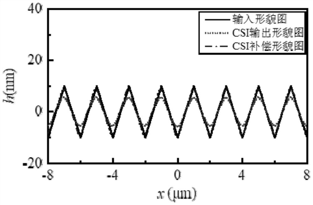
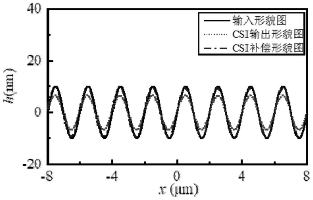
[0058] Such as figure 1 As shown, the high-frequency shape compensation method of the white light scanning interferometry method based on the transfer function of the present invention, the specific compensation steps are: the initial shape measured by the white light interferometer, and the Fourier transform of the shape is solved to obtain the phase frequency curve and amplitude-frequency curve, solve the PSD of the power spectral density curve for the amplitude-frequency curve, use the transfer function to obtain the corrected PSD, and combine the corrected PSD and the phase-frequency curve to obtain the compensation shape by using the inverse periodogram method.
[0059] The present invention adopts software to carry out measurement process simulation simulation and compensation, and concrete method is as follows:
[0060] S1: Given the triangular wave signal to simulate the shape, use mathematical software combined with the white light interferometry process to simulate t...
Embodiment 2
[0064] The New view 9000 white light scanning interferometer of ZYGO Company was used to measure the morphology of No. 3000 ultra-precision ground silicon wafers, such as Image 6 As shown in (a), use mathematical software to randomly extract k groups (k=20) of two-dimensional profile curves with a length of 20 μm from the vertical wear scar direction, and use mathematical software to extract the power spectral density curve PSD of the above-mentioned shape Ci , wherein i=1, 2, 3, ..., k, adopt the XE-200 atomic force microscope of Park Systems Company to measure the morphology of the same No. 3000 ground silicon wafer sample, as Image 6 As shown in (b), use mathematical software to randomly extract k groups (k=20) of two-dimensional profile curves with a length of 20 μm from the vertical wear scar direction, and use mathematical software to extract the power spectral density curve PSD of the above-mentioned shape Ai , to calculate the average power spectral density curves me...
PUM
| Property | Measurement | Unit |
|---|---|---|
| length | aaaaa | aaaaa |
| surface roughness | aaaaa | aaaaa |
| surface roughness | aaaaa | aaaaa |
Abstract
Description
Claims
Application Information


