Defect detection wafer graph optimization method and optimization system thereof

A defect detection and optimization method technology, applied in semiconductor/solid-state device testing/measurement, electrical components, semiconductor/solid-state device manufacturing, etc., can solve problems such as flooding, low value, large quantity, etc., to save time and release machines The effect of increasing production capacity and reducing manpower consumption

Pending Publication Date: 2021-05-14
SHANGHAI HUALI MICROELECTRONICS CORP
View PDF8 Cites 2 Cited by
  • Summary
  • Abstract
  • Description
  • Claims
  • Application Information

AI Technical Summary

Problems solved by technology

[0002] During the defect detection process, it was found that the wafer edge defect count (total amount of defects on the wafer edge) was relatively high, including defects (defects) caused by litho (lithography) defocus (out of focus) and CMP (chemical mechanical planarization) and TF ( Discolor (plastic package discoloration) and other defects caused by plastic package cutting), the number of such defects is relatively large, and some of them are located in chips that do not need needle testing in the future (that is, invalid chips, which are of low value and are usually discarded), which will cause Other key defects (defects on effective chips) are submerged in it and cannot be effectively alarmed, and subsequent defect detection sites can be caught (detected), which will affect the monitor of multiple processes (procedures).

Method used


Image

  • Defect detection wafer graph optimization method and optimization system thereof
  • Defect detection wafer graph optimization method and optimization system thereof
  • Defect detection wafer graph optimization method and optimization system thereof

Examples


Embodiment Construction

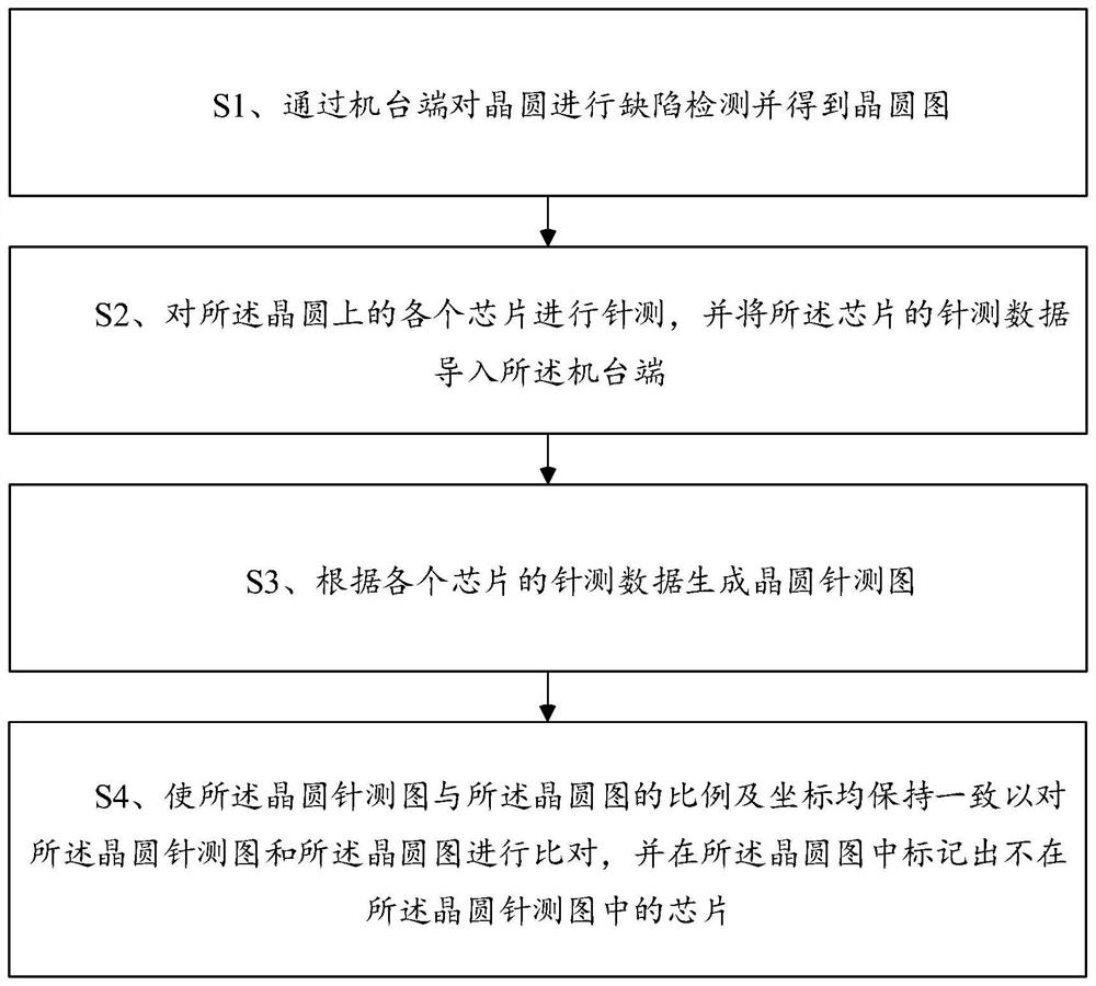
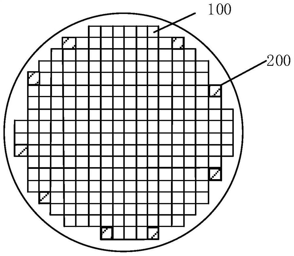
[0034] As mentioned in the background technology, since there are many defects on invalid chips that do not need pin testing, and it is easy to affect the defect detection of valid chips, in order to avoid the influence of such defects, at present, mainly by referring to the scan map (wafer map) in the ACE software ) is compared with the CP map (wafer probe map), and the chip (invalid chip) that does not measure the CP is marked (marked) by manual operation on the software interface and removed. This method has a great influence of human factors, and there will be false marks. The phenomenon.

[0035] Based on this, the present invention provides a defect detection wafer map optimization method and its optimization system, which can automatically mark invalid chips directly on the defect detection machine side, optimize the wafer map, and avoid the influence of abnormal defects.

[0036] In order to make the purpose, advantages and features of the present invention clearer, th...


PUM


Abstract

The invention provides a defect detection wafer graph optimization method and an optimization system thereof. The defect detection wafer graph optimization method comprises the following steps of: performing defect detection on a wafer through a machine end to obtain a wafer graph; carrying out probe testing on each chip on the wafer, and importing probe testing data of the chips into the machine end; generating a wafer probing map according to the probing data of each chip; and making the proportion and coordinates of the wafer prober map and the wafer map consistent so as to compare the wafer prober map and the wafer map, and marking chips which are not in the wafer prober map in the wafer map. According to the defect detection wafer graph optimization method, the prober data is imported into the machine end, the wafer prober map is generated, the wafer prober map is compared with the wafer map of the machine end, invalid chips can be marked efficiently and accurately, optimization of the wafer map is achieved, the capacity of the machine is released, time is saved, and manpower consumption is reduced.

Description

technical field [0001] The invention relates to the technical field of semiconductor defect detection, in particular to a defect detection wafer map optimization method and an optimization system thereof. Background technique [0002] During the defect detection process, it was found that the wafer edge defect count (total amount of defects on the wafer edge) was relatively high, including defects (defects) caused by litho (lithography) defocus (out of focus) and CMP (chemical mechanical planarization) and TF ( Discolor (plastic package discoloration) and other defects caused by plastic package cutting), the number of such defects is relatively large, and some of them are located in chips that do not need needle testing in the future (that is, invalid chips, which are of low value and are usually discarded), which will cause Other key defects (defects on effective chips) are submerged in it and cannot be effectively alarmed, and subsequent defect detection sites can be caugh...

Claims


Application Information

Patent Timeline
Patent Type & Authority Applications(China)
IPC IPC(8): H01L21/66H01L21/67
CPCH01L22/12H01L22/14H01L22/20H01L21/67288H01L21/67282
Inventor 汪金凤
Owner SHANGHAI HUALI MICROELECTRONICS CORP
Why Eureka
Try Eureka