Semiconductor device heat dissipation structure and preparation method thereof

A heat dissipation structure and semiconductor technology, applied in semiconductor devices, semiconductor/solid-state device manufacturing, semiconductor/solid-state device components, etc., can solve problems such as large thermal resistance and poor heat dissipation

Active Publication Date: 2021-05-14
度亘核芯光电技术(苏州)有限公司
View PDF6 Cites 0 Cited by
  • Summary
  • Abstract
  • Description
  • Claims
  • Application Information

AI Technical Summary

Problems solved by technology

[0004] The purpose of the present invention is to provide a semiconductor device heat dissipation structure and its preparation method to solve the technical problems in the prior art that the semiconductor device heat dissipation structure has a large thermal resistance and poor heat dissipation effect

Method used


Image

  • Semiconductor device heat dissipation structure and preparation method thereof
  • Semiconductor device heat dissipation structure and preparation method thereof
  • Semiconductor device heat dissipation structure and preparation method thereof

Examples


Embodiment Construction

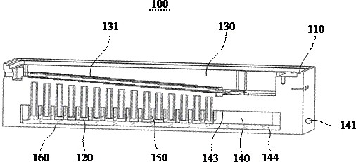
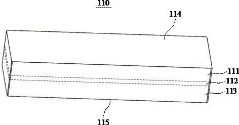
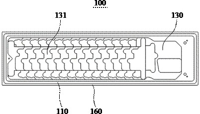
[0038] In order to make the purpose, technical solutions and advantages of the embodiments of the present invention clearer, the technical solutions in the embodiments of the present invention will be clearly and completely described below in conjunction with the drawings in the embodiments of the present invention. Obviously, the described embodiments It is a part of embodiments of the present invention, but not all embodiments. The components of the embodiments of the invention generally described and illustrated in the figures herein may be arranged and designed in a variety of different configurations. Accordingly, the following detailed description of the embodiments of the invention provided in the accompanying drawings is not intended to limit the scope of the claimed invention, but merely represents selected embodiments of the invention. Based on the embodiments of the present invention, all other embodiments obtained by persons of ordinary skill in the art without cre...


PUM


Abstract

The invention discloses a semiconductor device heat dissipation structure and a preparation method thereof, the semiconductor device heat dissipation structure comprises a composite shell and a heat pipe arranged in the composite shell, and the composite shell comprises an integrated structure formed by sequentially superposing a heat absorption material layer, a transition material layer and a heat dissipation material layer; the transition material layer is formed by mutual diffusion of atoms of the heat absorption material layer and the heat dissipation material layer, a device installation part is arranged on the surface, located on one side of the heat absorption material layer, of the composite shell, the bottom face of the device installation part is used for arranging a semiconductor device, and a cavity used for circulation of a cooling medium is formed in the heat dissipation material layer, the composite shell and the pipe wall of the heat pipe are of an integrated structure, and the side, opposite to the bottom face of the device installation part, of the heat pipe extends towards the interior of the cavity. The semiconductor device heat dissipation structure is of an integrated structure and is not provided with a contact interface with high thermal resistance, heat generated by the semiconductor device can be rapidly dissipated through multiple heat dissipation means, the size of the semiconductor device heat dissipation structure is not increased, and the requirement of a miniaturized device can be met.

Description

technical field [0001] The invention relates to the technical field of semiconductors, in particular to a heat dissipation structure of a semiconductor device and a preparation method thereof. Background technique [0002] With the further development of science and technology, semiconductor technology, information technology and other cutting-edge technology fields are developing towards high power, high integration and miniaturization, resulting in the continuous increase of the heat dissipated by the system, and the high power density semiconductor devices inside the system continue to challenge the limit of its cooling system. [0003] In the prior art, a simple air-cooled or liquid-cooled heat dissipation system is usually used to cool down semiconductor devices. The heat dissipation efficiency of this type of heat dissipation system is low, and the liquid-cooled heat dissipation system usually has multiple component structures. Different component structures There wil...

Claims


Application Information

Patent Timeline
Patent Type & Authority Applications(China)
IPC IPC(8): H01L23/427H01L23/46H01L23/373H01L21/48
CPCH01L21/4803H01L23/3735H01L23/427H01L23/46
Inventor 赵卫东惠利省李靖卢乐杨国文
Owner 度亘核芯光电技术(苏州)有限公司
Why Eureka
Try Eureka